
Fabrication method of thin metal layer photolithography alignment mark

A thin metal layer, photolithographic alignment technology, applied in the direction of electrical components, electrical solid devices, circuits, etc., can solve problems that affect product performance, deviation, and easy alarms, etc., to improve alignment accuracy and improve height difference and contrast between light and dark, to ensure the effect of design performance

Active Publication Date: 2015-12-02
SHANGHAI HUAHONG GRACE SEMICON MFG CORP
View PDF6 Cites 0 Cited by
  • Summary
  • Abstract
  • Description
  • Claims
  • Application Information

AI Technical Summary

Problems solved by technology

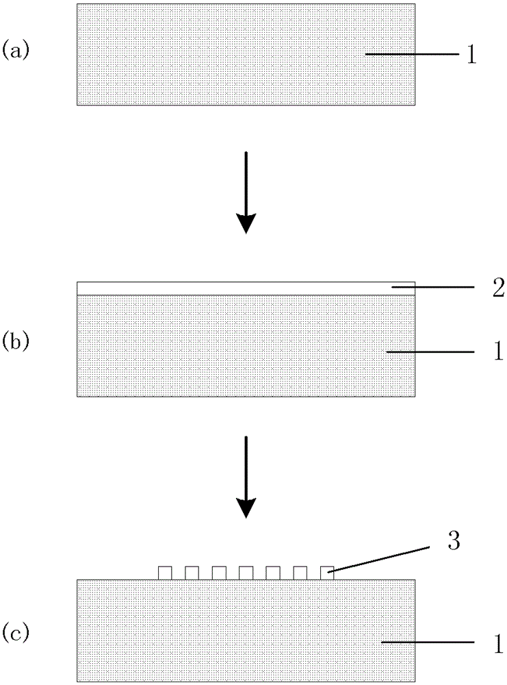
However, this indirect alignment method has the following disadvantages: 1. The alignment stability is poor. If the front and front layer marks are affected in the thin metal layer process, an alarm will easily occur when the rear layer is aligned; 2. , When the direction of the alignment compensation value of the thin metal layer is opposite to that of the subsequent layer, the alignment will be deviated, which will increase the rework rate of the product and even affect the performance of subsequent products

Method used


Image

  • Fabrication method of thin metal layer photolithography alignment mark
  • Fabrication method of thin metal layer photolithography alignment mark
  • Fabrication method of thin metal layer photolithography alignment mark

Examples


Embodiment Construction

[0020] In order to have a more specific understanding of the technical content, characteristics and effects of the present invention, now in conjunction with the illustrated embodiment, the details are as follows:

[0021] The manufacturing method of the photolithographic alignment mark of the thin metal layer in this embodiment has a specific process flow as follows:

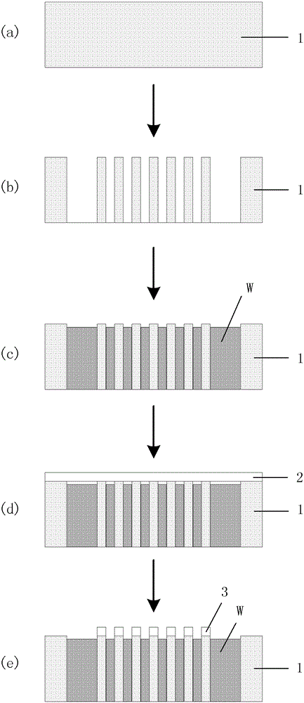
[0022] Step 1, laying down the dielectric layer 1 under the thin metal layer 2, such as image 3 as shown in (a);

[0023] Step 2, on the dielectric layer 1, at the position corresponding to the photolithographic alignment mark 3 of the thin metal layer 2 to be fabricated, apply photoresist, then expose to light, and etch away the area not blocked by the photoresist, Such as image 3 (b) shown.

[0024] Step 3, fill the area etched in step 2 with tungsten (W). In this step, other metals or alloys can also be used for filling, but the filling material cannot be the same as that of the thin metal layer.

[0...


PUM

PropertyMeasurementUnit
thicknessaaaaaaaaaa

Abstract

The invention discloses a method for manufacturing photoetching alignment marks for thin metal layers. Before depositing of a thin metal layer, the method further includes the steps of firstly, coating photoresist to the position of a substrate dielectric layer, corresponding to a photoetching alignment mark to be made, to form a barrier layer, exposing and etching; secondly, filling a region etched in the step 1 with metal or alloy different from the material of the thin metal layer; and thirdly, subjecting the surface of the filled region to chemical mechanical polishing to allow the surface to be lower than the dielectric layer. Height difference and brightness contrast of the photoetching alignment mark for the thin metal layer are improved by changing the substrate structure of the photoetching alignment mark for the thin metal layer, so that direct alignment of a late layer with the thin metal layer is achieved, precision in aligning the previous layer and the late layer is improved and production design performance is improved.

Description

technical field [0001] The invention relates to the field of semiconductor manufacturing, in particular to a method for manufacturing a thin metal layer photolithography alignment mark. Background technique [0002] In the semiconductor manufacturing process, the alignment accuracy of lithography is one of the key factors restricting the process of smaller dimensions. Due to the correlation between the front and rear layers of the layout design, in the subsequent process, the method of directly aligning the photolithographic alignment marks of the front layer with the rear layer is usually used to improve the alignment accuracy of the front and rear layers and ensure the performance of the product. [0003] In some special process platforms, a thin metal layer will be introduced in the subsequent process to connect the upper and lower dielectric layers. For example, in the self-alignment process introduced in the embedded flash (Embedded Flash) process platform, the key ste...

Claims


Application Information

Patent Timeline
Patent Type & Authority Patents(China)
IPC IPC(8): H01L23/544
Inventor 童宇锋李伟峰陈福成
Owner SHANGHAI HUAHONG GRACE SEMICON MFG CORP
Learn More