
Method for manufacturing polydimethylsiloxane (PDMS) film with integrated microstructure

A technology of PDMS and production method, which is applied in the field of microfluidic chip and membrane separation, can solve the problems that PDMS film can not be used flexibly alone, and achieve the effect of ensuring flatness, reducing operation difficulty and avoiding wrinkles

Active Publication Date: 2013-04-03
SHANGHAI INST OF MICROSYSTEM & INFORMATION TECH CHINESE ACAD OF SCI
View PDF4 Cites 28 Cited by
  • Summary
  • Abstract
  • Description
  • Claims
  • Application Information

AI Technical Summary

Problems solved by technology

Although this method improves the success rate of peeling off the PDMS thin film structure by superimposing a support layer with high strength and reduces the difficulty of the peeling operation of the PDMS thin film structure, the PDMS thin film produced has relatively large limitations in application, because the The prepared PDMS film is bonded with another thick PDMS structural block, the two must be applied together as a whole, and the independent flexible application of the PDMS film cannot be realized

Method used


Image

  • Method for manufacturing polydimethylsiloxane (PDMS) film with integrated microstructure
  • Method for manufacturing polydimethylsiloxane (PDMS) film with integrated microstructure
  • Method for manufacturing polydimethylsiloxane (PDMS) film with integrated microstructure

Examples


specific Embodiment approach

[0019] A PDMS film with an integrated high-density micro-through-hole array is prepared by using the integrated microstructure PDMS film manufacturing method proposed by the present invention, which is applied to cell patterned fixed growth. The specific implementation is as follows:

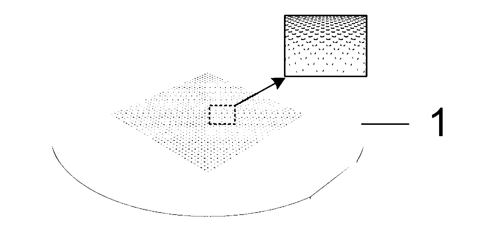
[0020] 1. Make the SU-8 micro-column array structure on the silicon wafer by photolithography, and complete the preparation of the master mold 1 (such as figure 1 shown);

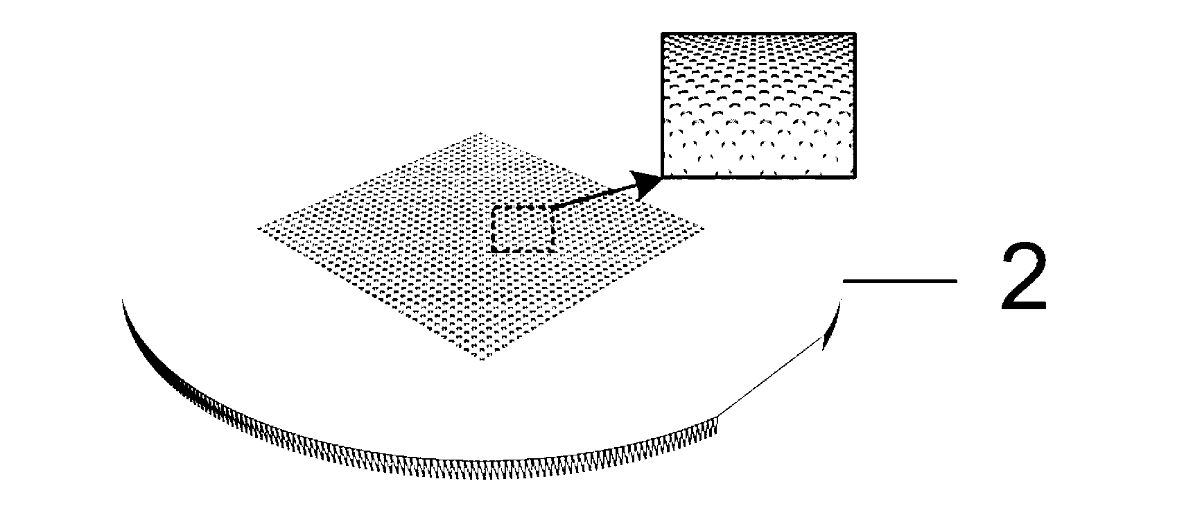
[0021] 2. Pouring the mixed solution of PDMS prepolymer and curing agent (10:1, w / w) on the master mold 1 made of silicon wafer and SU-8, heating and curing, and peeling off to obtain the reverse mold 2 of PDMS ( Such as figure 2 shown);

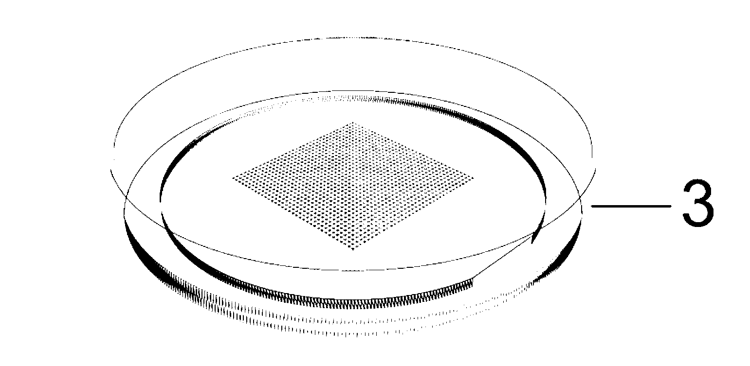
[0022] 3. Place the prepared PDMS reverse mold 2 with the structure facing upwards, attach it to the bottom 3 of the petri dish, and pour a hot-dissolved agarose solution (such as image 3 shown), after the agarose is cooled and solidified, the excess agarose on the edge is cut off, an...


PUM

PropertyMeasurementUnit
Thicknessaaaaaaaaaa

Abstract

The invention discloses a method for manufacturing a polydimethylsiloxane (PDMS) film with an integrated microstructure. The method is characterized in that firstly a PDMS rotary die technology is utilized to replicate a targeted microstructure from a female die manufactured based on micro-processing technology to the surface of a hot melting or water soluble material so as to form a sacrificial layer die with a meltable or dissolution characteristic; and then the surface of the manufactured sacrificial layer die is coated with a thin layer of PDMS rotationally, simultaneously an outer film frame is attached to the PDMS in a pressing manner, finally a PDMS film structure is released through hearing or smelting in water or dissolving the sacrificial layer die after the PDMS is cured, and the transferring and application of the PDMS film are achieved with the assistance of the outer film frame. The method utilizes the sacrificial layer die to manufacture and release the PDMS film with the integrated structure, prevents traditional manual mechanical peeling methods from damaging the PDMS film, substantially reduces difficulty in manufacturing of fragile PDMS film structure, increases the success rate of manufacturing the PDMS film and can achieve the high-yield mass production of the PDMS film structure.

Description

technical field [0001] The invention relates to a method for manufacturing a PDMS thin film with an integrated microstructure, which can be applied to the technical fields of microfluidic chips and membrane separation. Background technique [0002] PDMS is a common organic material. It is colorless, odorless, stable in chemical properties, low in price, easy to process, and has good light transmittance and biocompatibility. Therefore, thin films based on PDMS materials are used in microfluidic chips. It has a wide range of applications in the field and membrane separation technology. Especially in microfluidic chips, PDMS films can be used to make components such as microvalves, peristaltic micropumps, and adjustable microlenses; in addition, PDMS films can also be used in artificial skin for tissue engineering, patterned modification of curved surfaces, etc. aspect. At present, there are usually two traditional methods for making PDMS films: one is to spin-coat PDMS on th...

Claims


Application Information

Patent Timeline
IPC IPC(8): B29C41/04B29C33/38B29C41/34B29L7/00
Inventor 李刚汤腾赵建龙
Owner SHANGHAI INST OF MICROSYSTEM & INFORMATION TECH CHINESE ACAD OF SCI
Learn More