Electroplating process of circuit board of burning-resistant board
An electroplating process and circuit board technology, applied in jewelry, etc., can solve the problems of electroplating layer thickness, copper layer thickness, burning board, etc., and achieve the effects of maintaining bonding force and structural cohesion, reducing electroplating area, and uniform current
- Summary
- Abstract
- Description
- Claims
- Application Information
AI Technical Summary
Problems solved by technology
Method used
Image

Examples
Embodiment 1
[0028] A circuit board electroplating process for a burn-proof board, which includes providing a substrate, covering a copper foil layer around the front surface of the substrate, and then performing the following steps:
[0029] Drilling: The drilling speed of the drill bit is 18000-20000 rpm.
[0030] The first grinding plate: the grinding plate speed is 40-60dm / min, the brushing current is 3.0-4.0A, and the pickling pressure is 0.5-1.5kg / cm 2 , the pickling pressure is 0.5-1.5 kg / cm 2 , the overflow washing pressure is 0.5-1.5 kg / cm 2 , pressurized water washing pressure is 1-2kg / cm 2 , high pressure washing pressure is 10-15kg / cm 2 , ultra-high pressure washing pressure is 60-805kg / cm 2 , The drying temperature is 70-90 ℃.
[0031] Copper sinking: use the chemical copper sinking method to deposit chemical copper on the surface of the board and in the holes, with a thickness of 3-5um.
[0032] The second grinding plate: the grinding plate speed is 25-35 kg / cm 2 , hig...
Embodiment 2
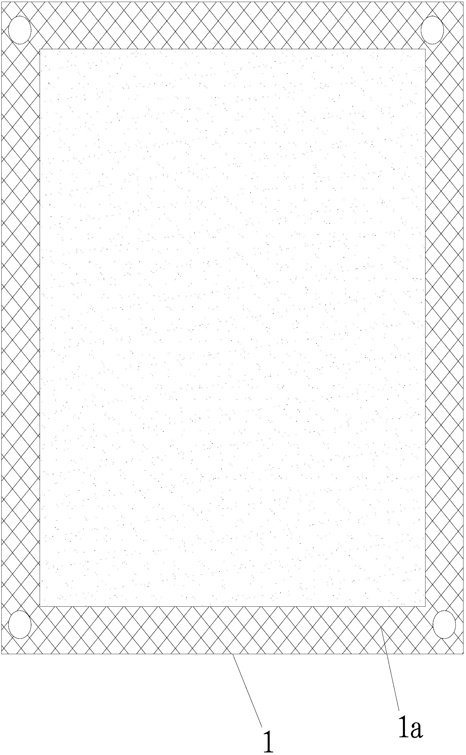
[0037] A circuit board electroplating process for a burn-proof board, which includes providing a substrate 1, a copper foil layer 1a is provided around the board surface of the substrate 1, and the copper foil layer 1a is a grid structure, and the grid structure The length of each hollow space is 0.3mm, and the width is 0.3mm, such as figure 1 shown, and then perform the following steps:
[0038] Drilling: The drilling speed of the drill bit is 18000-20000 rpm.
[0039] The first grinding plate: the grinding plate speed is 40-60dm / min, the brushing current is 3.0-4.0A, and the pickling pressure is 0.5-1.5kg / cm 2 , the pickling pressure is 0.5-1.5 kg / cm 2 , the overflow washing pressure is 0.5-1.5 kg / cm 2 , pressurized water washing pressure is 1-2kg / cm 2 , high pressure washing pressure is 10-15kg / cm 2 , ultra-high pressure washing pressure is 60-805kg / cm 2 , The drying temperature is 70-90 ℃.
[0040] Copper sinking: use the chemical copper sinking method to deposit ch...
Embodiment 3
[0046]A circuit board electroplating process for a burn-proof board, which includes providing a substrate, and a copper foil layer is provided around the board surface of the substrate, and the copper foil layer is a grid structure, and each hollow of the grid structure The length of the grid is 0.3mm, the width is 0.3mm, and then the following steps are performed:
[0047] Drilling: The drilling speed of the drill bit is 18000-20000 rpm.
[0048] The first grinding plate: the grinding plate speed is 40-60dm / min, the brushing current is 3.0-4.0A, and the pickling pressure is 0.5-1.5kg / cm 2 , the pickling pressure is 0.5-1.5 kg / cm 2 , the overflow washing pressure is 0.5-1.5 kg / cm 2 , pressurized water washing pressure is 1-2kg / cm 2 , high pressure washing pressure is 10-15kg / cm 2 , ultra-high pressure washing pressure is 60-805kg / cm 2 , The drying temperature is 70-90 ℃.
[0049] Copper sinking: use the chemical copper sinking method to deposit chemical copper on the sur...
PUM
| Property | Measurement | Unit |
|---|---|---|
| length | aaaaa | aaaaa |
| width | aaaaa | aaaaa |
Abstract
Description
Claims
Application Information
 - R&D
- Intellectual Property
- Life Sciences
- Materials
- Tech Scout
- Unparalleled Data Quality
- Higher Quality Content
- 60% Fewer Hallucinations
Browse by: Latest US Patents, China's latest patents, Technical Efficacy Thesaurus, Application Domain, Technology Topic, Popular Technical Reports.
© 2025 PatSnap. All rights reserved.Legal|Privacy policy|Modern Slavery Act Transparency Statement|Sitemap|About US| Contact US: help@patsnap.com