Power semiconductor device
A semiconductor and power technology, applied in the direction of semiconductor devices, electrical components, circuits, etc., can solve the problems of impurity injection amount deviation, withstand voltage reduction, etc., and achieve the effect of suppressing withstand voltage reduction
- Summary
- Abstract
- Description
- Claims
- Application Information
AI Technical Summary
Problems solved by technology
Method used
Image
Examples
no. 1 Embodiment approach
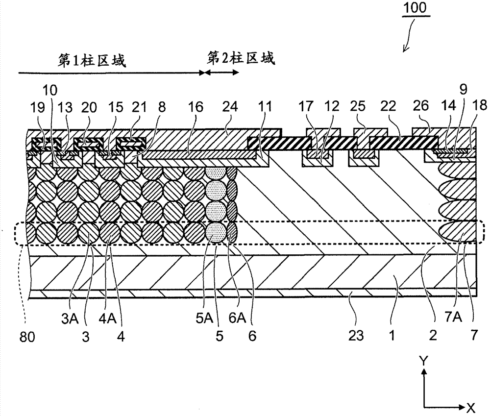
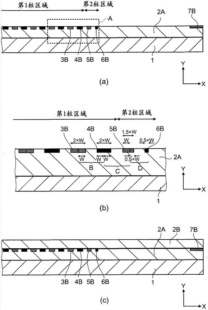
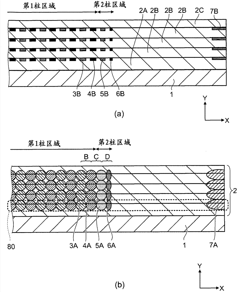
[0028] use Figure 1 to Figure 5 , the power semiconductor device according to the first embodiment of the present invention will be described. figure 1 It is a schematic sectional view of main parts of the power semiconductor device according to the first embodiment. figure 2 It is a figure which shows a part of the manufacturing process of the power semiconductor device of 1st Embodiment, (a) is a main part schematic cross-sectional view, (b) is an enlarged view of A part in (a), (c) is ( a) Schematic cross-sectional view of the main part of the subsequent process. image 3 It is a figure showing a part of the manufacturing process of the power semiconductor device of 1st Embodiment, (a) is a main part schematic cross-sectional view, (b) is a main part schematic cross-sectional view of the process after (a). Figure 4 It is a figure which shows a part of the manufacturing process of the power semiconductor device of a comparative example, and is the same as figure 2 (b)...
no. 2 Embodiment approach
[0068] use Figure 6 as well as Figure 7 , the power semiconductor device 200 of the second embodiment will be described. Figure 6 It is a schematic cross-sectional view of a main part of a power semiconductor device according to a second embodiment. Figure 7 It is a figure which shows part of the manufacturing process of the power semiconductor device of 2nd Embodiment, (a) is a main part schematic cross-sectional view, (b) is an enlarged view of the F part in (a). In addition, the same reference numerals or signs are assigned to the same configurations as those described in the first embodiment, and description thereof will be omitted. Differences from the first embodiment will be mainly described.
[0069] Such as Figure 6 As shown, the MOSFET 200 of the second embodiment, like the MOSFET 100 of the first embodiment, includes a high-resistance epitaxial layer 2 having a first pillar region and a second pillar region as n - shape drift layer. In the second column r...
no. 3 Embodiment approach
[0078] use Figure 8 as well as Figure 9 , the power semiconductor device 300 of the third embodiment will be described. Figure 8 It is a schematic sectional view of a main part of a power semiconductor device according to a third embodiment. Figure 9 It is a figure which shows part of the manufacturing process of the power semiconductor device of 3rd Embodiment, (a) is a main part schematic cross-sectional view, (b) is an enlarged view of G part in (a). In addition, the same reference numerals or symbols are assigned to the same components as those described in the first embodiment, and description thereof will be omitted. Differences from the first embodiment will be mainly described.
[0079] Such as Figure 8 As shown, the MOSFET 300 of the third embodiment, like the MOSFET 100 of the first embodiment, includes a high-resistance epitaxial layer 2 having a first pillar region and a second pillar region as n - shape drift layer. The second column region of the MOSFE...
PUM
 Abstract
Description
Claims
Application Information
 - R&D
- Intellectual Property
- Life Sciences
- Materials
- Tech Scout
- Unparalleled Data Quality
- Higher Quality Content
- 60% Fewer Hallucinations
Browse by: Latest US Patents, China's latest patents, Technical Efficacy Thesaurus, Application Domain, Technology Topic, Popular Technical Reports.
© 2025 PatSnap. All rights reserved.Legal|Privacy policy|Modern Slavery Act Transparency Statement|Sitemap|About US| Contact US: help@patsnap.com


