Light emitting diode (LED) aluminum substrate and manufacturing method thereof

A technology of LED aluminum substrate and manufacturing method, which is applied in the direction of electrical components, circuits, semiconductor devices, etc., can solve problems such as tight lamination and shedding of circuit layers, and achieve the effects of improving light extraction efficiency, good reflection, and increasing friction coefficient

Active Publication Date: 2013-04-10
HONGLI ZHIHUI GRP CO LTD
View PDF4 Cites 5 Cited by
  • Summary
  • Abstract
  • Description
  • Claims
  • Application Information

AI Technical Summary

Problems solved by technology

At present, in the LED industry, COB boards made of mirror aluminum substrates are made of a whole piece of mirror aluminum substrate without any surface treatment. The mirror functional area and non-functional area are smooth, and the entire aluminum substrate is smooth. , although a very good light reflection efficiency is achieved, when the circuit layer is pressed in the line pressing area, because the surface of the mirror aluminum is relatively smooth, the circuit layer is not pressed tightly, and it is easy to fall off.

Method used


Image

  • Light emitting diode (LED) aluminum substrate and manufacturing method thereof
  • Light emitting diode (LED) aluminum substrate and manufacturing method thereof
  • Light emitting diode (LED) aluminum substrate and manufacturing method thereof

Examples


Embodiment Construction

[0025] The present invention will be further described below in conjunction with the accompanying drawings of the description.

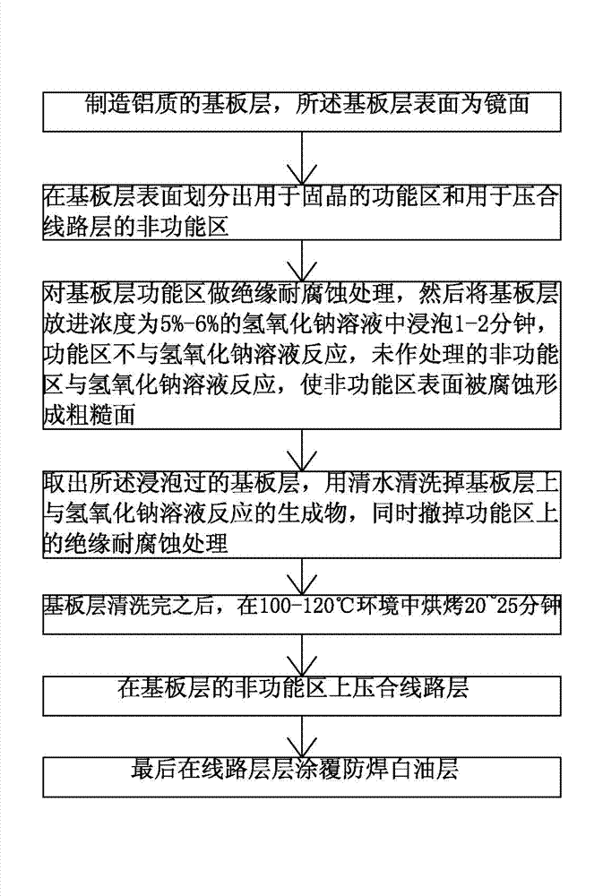
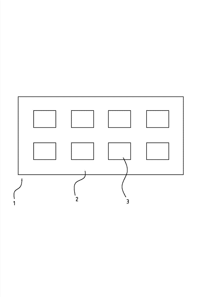
[0026] Such as Figures 1 to 3 Shown, a kind of LED aluminum substrate, its manufacturing method comprises the following steps:

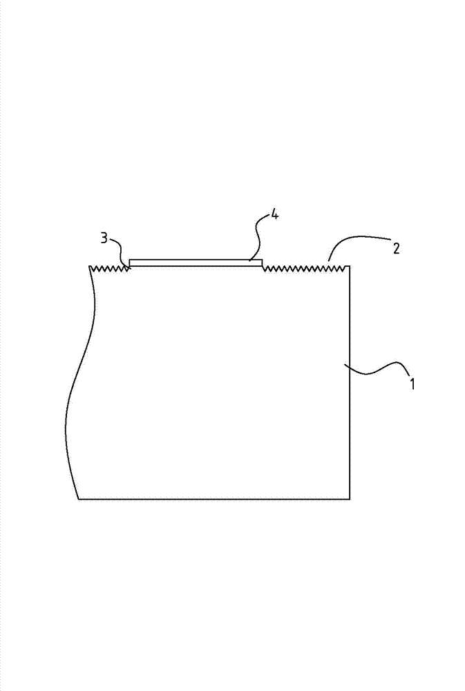
[0027] (1) Manufacturing an aluminum substrate layer 1, the substrate layer 1 is a mirror aluminum substrate, so that the surface of the substrate layer 1 is a smooth mirror surface;

[0028] (2) Use film on the surface of the substrate layer 1 to divide the functional area 3 for die bonding and the non-functional area 2 for laminating the circuit layer;

[0029] (3) Perform insulation and corrosion resistance treatment on the functional area 3 of the substrate layer 1, first brush the blue oil on the functional area 3, and paste the blue film 4 on the area covered with the blue oil; the main components of the blue oil and the blue film 4 It is saturated hydrocarbon polyester, polyethylene or polypropylene, and d...


PUM


Abstract

The invention provides a light emitting diode (LED) aluminum substrate. A manufacturing method for the LED aluminum substrate includes the following steps of manufacturing the substrate layer, dividing functional zone and a non-functional zone on the surface of the substrate layer, doing isolation and corrosion resisting treatment to the functional zone of the substrate layer, then putting the substrate layer into 5%-6% sodium hydroxide solution to soak the substrate layer for 1-2 minutes, wherein the functional zone does not act with the sodium hydroxide solution, the non-functional zone acts with the sodium hydroxide solution, and surface of the non-functional zone is corroded to form a rough surface, taking out the soaked substrate layer, washing off sundries on the substrate layer through clear water, simultaneously removing the isolation and corrosion resisting treatment on the functional zone, baking the substrate layer for 20-25 minutes at the temperature of 100-120 DEG C after finishing cleaning the substrate layer, doing press fit of a wire level on the non-functional zone of the substrate layer, and coating the wire layer with an anti-welding white oil layer. The wire layer can be pressed tightly under the condition that good reflection efficiency of the substrate layer is guaranteed.

Description

technical field [0001] The invention relates to the application field of LEDs, in particular to an aluminum substrate for carrying LEDs and a manufacturing method thereof. Background technique [0002] The existing COB (chip on board) board made of mirror aluminum substrate uses technology to divide the mirror functional area and non-functional area on the mirror aluminum substrate, and then make it into a COB board. The mirror functional area is the die-bonding area, and the non- The functional area is the line pressing area. At present, in the LED industry, COB boards made of mirror aluminum substrates are made of a whole piece of mirror aluminum substrate without any surface treatment. The mirror functional area and non-functional area are smooth, and the entire aluminum substrate is smooth. , although a very good light reflection efficiency is achieved, when the circuit layer is pressed in the line pressing area, because the surface of the mirror aluminum is relatively ...

Claims


Application Information

Patent Timeline
Patent Type & Authority Applications(China)
IPC IPC(8): H01L33/62H01L33/60
Inventor 毛卡斯石超周志勇王芝烨黄巍王跃飞周小泉吴乾
Owner HONGLI ZHIHUI GRP CO LTD
Why Eureka
Try Eureka