Semiconductor template substrate, light-emitting element using a semiconductor template substrate, and a production method therefor

一种半导体、发光器件的技术,应用在半导体/固态器件制造、半导体器件、电气元件等方向,能够解决发光器件性能降低、高漏电流、发光器件芯片产量减少等问题,达到简化制造工艺的效果

Inactive Publication Date: 2013-04-10
ENF TECH
View PDF4 Cites 15 Cited by
  • Summary
  • Abstract
  • Description
  • Claims
  • Application Information

AI Technical Summary

Problems solved by technology

However, the laser lift-off process induces thermal / mechanical deformation of the light emitting stack structure including the active layer
For example, due to different lattice constants and thermal expansion coefficients, mechanical stress occurs between the nitride semiconductor layer and the thick sapphire substrate. Since the vertical nitride semiconductor light-emitting element light-emitting device cannot withstand mechanical stress, the vertical nitride semiconductor emits light. The device is subjected to mechanical / thermal damage
[0005] As described above, when the thin films of the stacked light-emitting structure are damaged, high leakage current is caused, and in addition, the chip yield of the light-emitting device is greatly reduced, resulting in a decrease in the overall performance of the light-emitting device

Method used


Image

  • Semiconductor template substrate, light-emitting element using a semiconductor template substrate, and a production method therefor
  • Semiconductor template substrate, light-emitting element using a semiconductor template substrate, and a production method therefor
  • Semiconductor template substrate, light-emitting element using a semiconductor template substrate, and a production method therefor

Examples


Embodiment Construction

[0027] Hereinafter, embodiments of the present invention will be described in detail with reference to the accompanying drawings so that those skilled in the art can easily implement the embodiments.

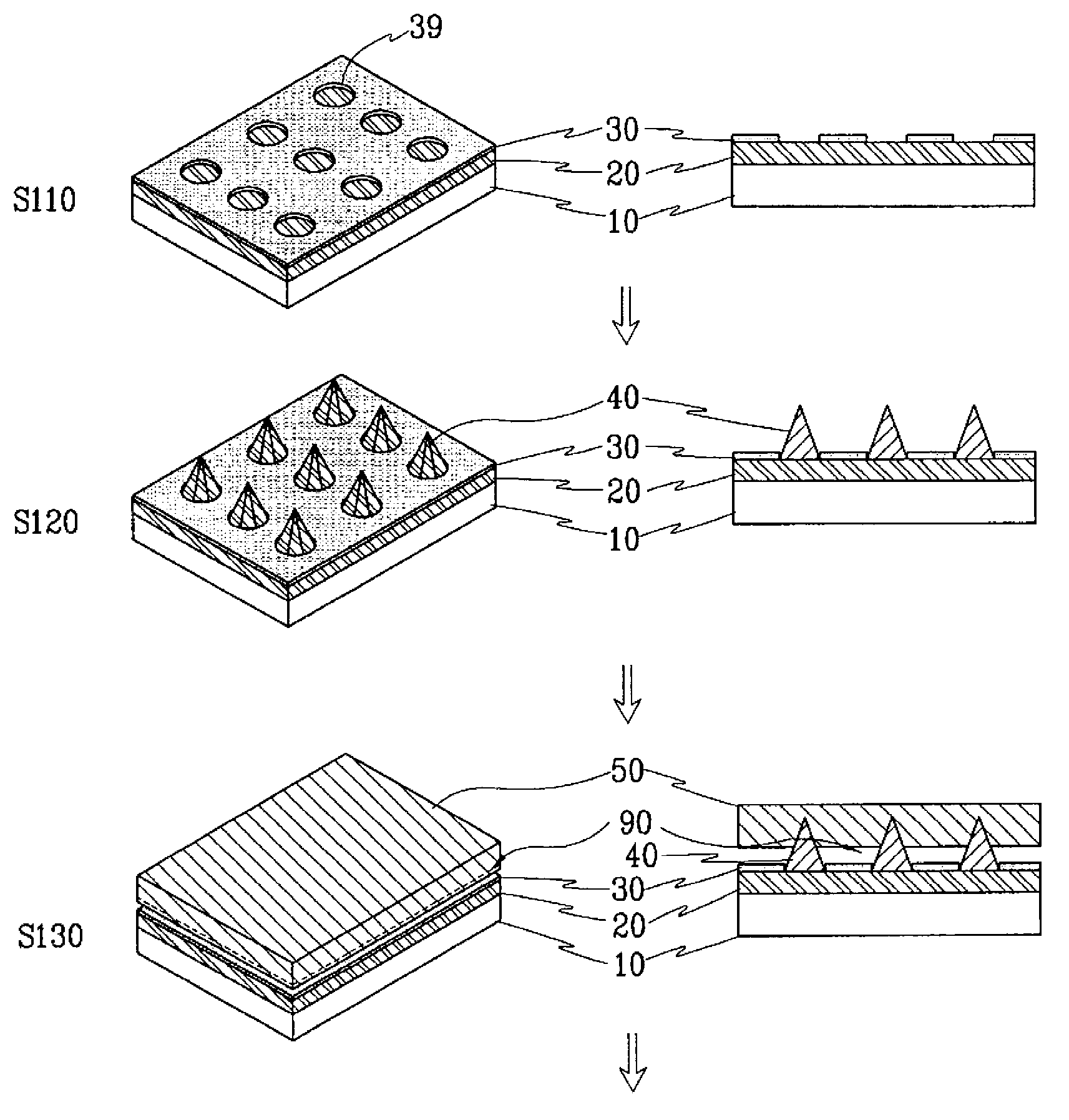
[0028] First, a semiconductor crystal manufacturing method according to an embodiment of the present invention will be described with reference to FIGS. 1A and 1B . For example, this embodiment is an embodiment in which n-type GaN crystals are grown using a sapphire substrate. However, materials used for the substrate and buffer layer, semiconductor layer, and light emitting stack structure are not limited thereto.

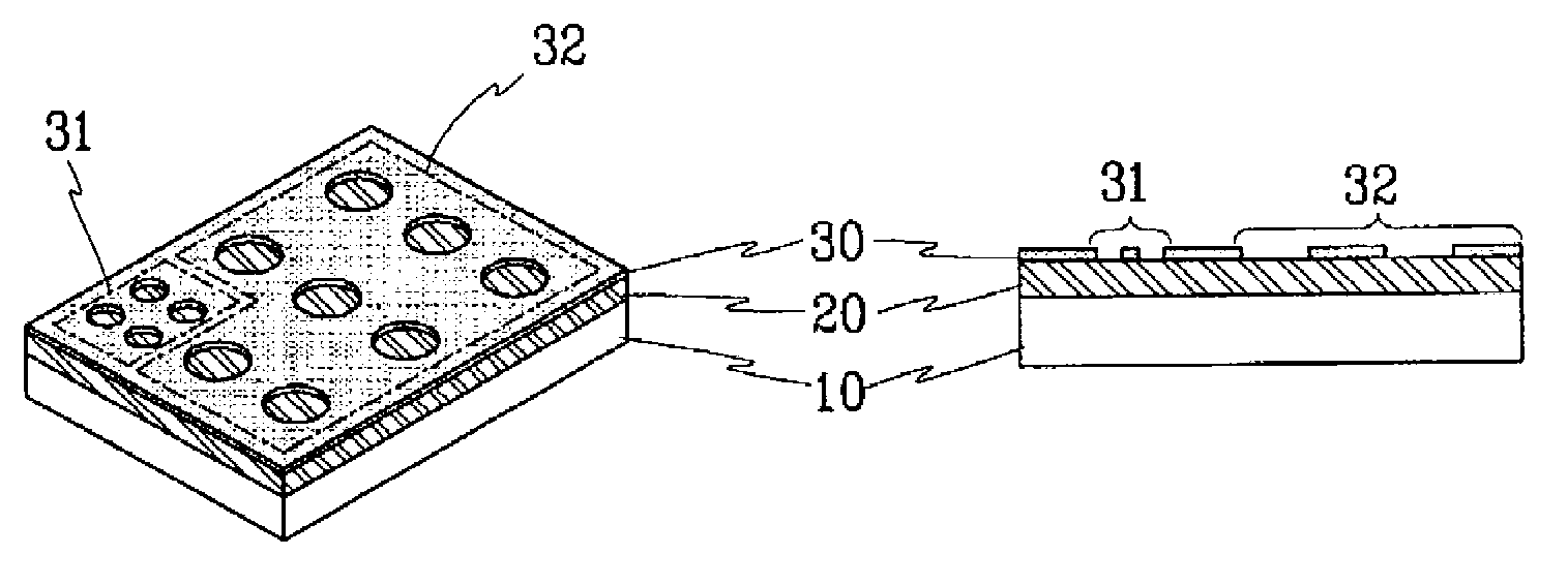
[0029] In operation S110 , a buffer layer 20 is formed on the insulating substrate 10 , and a mask layer 30 having a plurality of exposure patterns 39 is formed on the buffer layer 20 . In FIG. 1A , the exposure pattern 39 is shown in a circular shape. However, the exposure pattern 39 may be formed in a polygonal shape such as a quadrangle, a triangle, or a hexago...


PUM


Abstract

A light-emitting element comprises a semiconductor layer, a light-emitting laminated structure and a plurality of inverted pyramid structures formed in one surface of the light-emitting laminated structure. The transverse cross-sectional areas of the inverted pyramid structures decrease extending perpendicularly relative to the light-emitting laminated structure. The light-emitting element is rendered easier to produce due to the inverted pyramid structures.

Description

technical field [0001] The present invention relates to a semiconductor template substrate, a light-emitting device using the semiconductor template substrate, and a method for manufacturing the light-emitting device, and more particularly, to a semiconductor template substrate for reducing crystal defects and capable of being easily separated, using the semiconductor template substrate A light-emitting device at the bottom and a method for manufacturing the light-emitting device. Background technique [0002] Conventional semiconductor light emitting devices are formed as horizontal devices or vertical devices with an insulating substrate such as sapphire. For example, FIG. 6A shows a conventional horizontal semiconductor light emitting device, and FIG. 6B shows a conventional vertical semiconductor light emitting device. [0003] The horizontal semiconductor light emitting device includes a buffer layer 2 , an n-type nitride semiconductor layer 3 , an active layer 4 and a...

Claims


Application Information

Patent Timeline
Patent Type & Authority Applications(China)
IPC IPC(8): H01L33/22H01L21/20
CPCH01L33/007H01L21/0237H01L21/0242H01L21/02439H01L21/02458H01L21/0254H01L21/02642H01L21/0265H01L21/02664H01L33/12H01L33/0093
Inventor 安亨洙梁瑉河弘周
Owner ENF TECH
Why Eureka
Try Eureka