Surface mount microwave device and packaging process thereof

A microwave device and surface mount technology, which is applied in the manufacture of electric solid-state devices, semiconductor devices, semiconductor/solid-state devices, etc., can solve the problems of increasing packaging costs, inability to disassemble, reassemble or repair, etc., to increase and improve the application level Effective dielectric constant and distribution parameter elimination effect of circuit

Active Publication Date: 2013-04-17
成都泰格微电子研究所有限责任公司
View PDF3 Cites 7 Cited by
  • Summary
  • Abstract
  • Description
  • Claims
  • Application Information

AI Technical Summary

Problems solved by technology

When stamping embedded packaging is used, special stamping equipment is required to complete it,

Method used


Image

  • Surface mount microwave device and packaging process thereof
  • Surface mount microwave device and packaging process thereof
  • Surface mount microwave device and packaging process thereof

Examples


Embodiment Construction

[0034] The technical solution of the present invention will be further described in detail below in conjunction with the accompanying drawings, but the protection scope of the present invention is not limited to the following description.

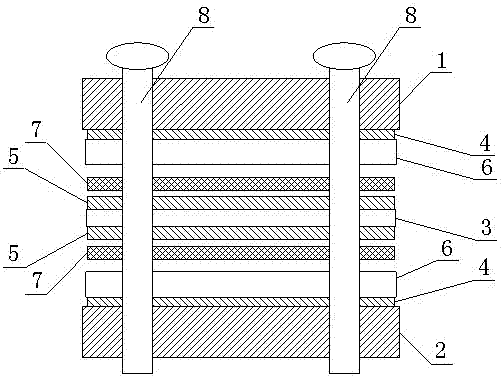
[0035] Such as figure 1 As shown, the surface mount microwave device includes an upper cover 1, a lower cover 2 and a central dielectric material layer 3, between the upper cover 1 and the central dielectric material layer 3, the lower cover 2 and the central dielectric material layer 3 The copper foil layer 4 and the copper foil circuit layer 5 are arranged symmetrically between them, the copper foil layer 4 is arranged on the side close to the upper and lower cover plates, and the copper foil circuit layer 5 is arranged on the side close to the central dielectric material layer 3, A dielectric material layer 6 is also provided between the copper foil layer 4 and the copper foil circuit layer 5 , and a laminated adhesive film layer 7 for l...


PUM


Abstract

The invention discloses a surface mount microwave device. Copper foil layers (4) and copper foil circuit layers (5) are symmetrically arranged between cover plates and a central medium material layer (3). Medium material layers (6) are arranged between the copper foil layers (4) and the copper foil circuit layers (5). Press-fitting glue film layers (7) for press-fitting are arranged between the copper foil circuit layers (5) and the medium material layers (6). A packaging process comprises the following steps of: tin paste printing, automatic mounting, curing, reflow soldering and cleaning to complete packaging. Since a strip line structure is used instead of a microstrip line and a copper foil circuit line in the strip line is in a folded and multilayer structure, the effective dielectric constant of the circuit is improved and the size of the microwave device is greatly reduced; and since a surface mount packaging method is adopted, slots for installation are not needed to be excavated in a printed circuit board and a chamber body, the printed circuit board is directly installed, the surface mounting is realized, the design and the realization of a microstrip circuit and a microstrip system are facilitated and optimized, the applicability is greatly increased and the application scope is wider.

Description

technical field [0001] The invention relates to a surface mounted microwave device and its packaging process. Background technique [0002] With the development of microwave technology, the design of microstrip circuits and systems has gradually become the design and application of transmission lines, monolithic microwave integrated circuits and microwave passive circuits. However, in many current designs, microwave devices cannot be directly mounted on the surface of the printed circuit board. Engineers have to directly design passive circuits on microstrip lines or design circuits into many modules, and then use coaxial connections. , but these methods lead to bulky equipment and complicated debugging tasks, which are not conducive to mass production of products, and cannot take advantage of the advantages of monolithic microwave integrated circuits. [0003] Traditional microwave devices adopt a single-layer microstrip line structure, the effective dielectric constant of...

Claims


Application Information

Patent Timeline
IPC IPC(8): H01L23/31H01L23/498H01L21/50H05K3/34
Inventor 吴永清邵高强
Owner 成都泰格微电子研究所有限责任公司
Why Eureka
Try Eureka