High-precision and pollution-free semiconductor wafer cleavage method

A semiconductor and pollution-free technology, applied in the field of high-precision and pollution-free semiconductor wafer cleavage, can solve problems such as difficult to clean and affect the quality of semiconductor wafers, and achieve the effect of improving chip quality and yield, and surface cleanliness

Inactive Publication Date: 2013-04-24
WUHAN TELECOMM DEVICES
View PDF12 Cites 6 Cited by
  • Summary
  • Abstract
  • Description
  • Claims
  • Application Information

AI Technical Summary

Problems solved by technology

The particle size of these debris is only about 1μm-10μm, which is difficult to clean and seriously affects the quality of semiconductor wafers after cleavage

Method used


Image

  • High-precision and pollution-free semiconductor wafer cleavage method
  • High-precision and pollution-free semiconductor wafer cleavage method
  • High-precision and pollution-free semiconductor wafer cleavage method

Examples


Embodiment Construction

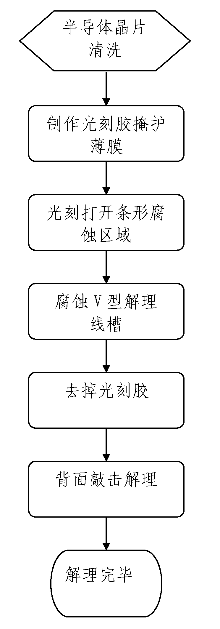
[0024] The present invention will be further described below in conjunction with the accompanying drawings and specific embodiments, so that those skilled in the art can better understand the present invention and implement it, but the examples given are not intended to limit the present invention.

[0025] The present invention proposes a high-precision and pollution-free semiconductor wafer cleavage method. As shown in FIG. The relative position of the back side of the cleavage line groove is knocked, so that the semiconductor wafer 1 is divided along the V-shaped cleavage line groove. As shown in Figure 2-Figure 8, it specifically includes the following steps:

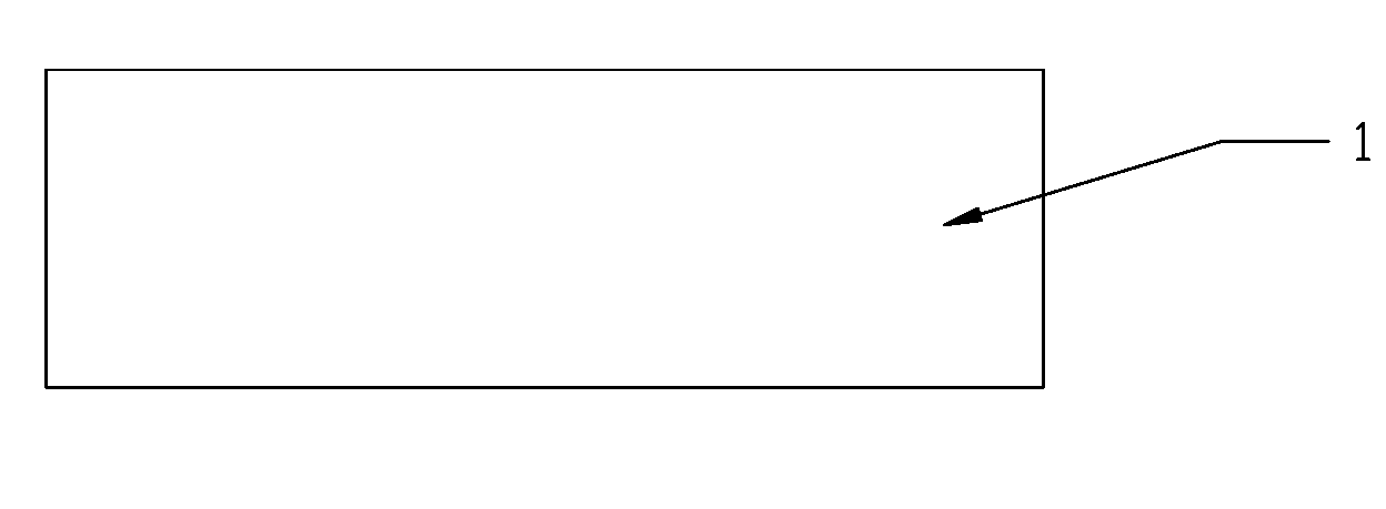
[0026] Step 1: As shown in FIG. 2 , the semiconductor wafer 1 to be cleaved is cleaned and blown dry with dry and clean nitrogen.

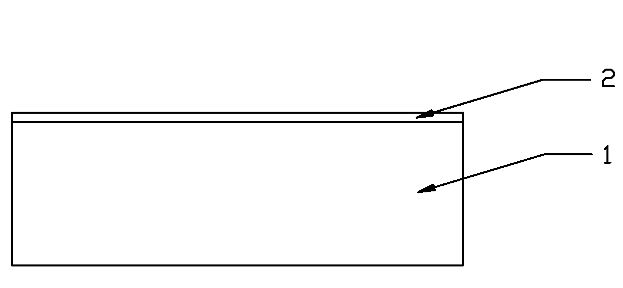
[0027] Step 2: Use photoresist 2 to make a protective film on the front side of semiconductor wafer 1. The photoresist 2 adopts ordinary positive photoresist, such as RZJ-304 positive ...


PUM

PropertyMeasurementUnit
thicknessaaaaaaaaaa

Abstract

The invention discloses a high-precision and pollution-free semiconductor wafer cleavage method. The method comprises the following steps: spinning photoresist on the surface of a semiconductor wafer to prepare a covering film; photoetching a strip-shaped run-through corrosion area on the covering film by using a photoetching machine; performing chemical corrosion in the corrosion area by using corrosive liquid to form a V-shaped cleavage slot; taking out the semiconductor wafer from the corrosive liquid and removing the covering film from the surface of the semiconductor wafer; and segmenting the semiconductor wafer along the V-shaped cleavage slot and finishing semiconductor wafer cleavage. The V-shaped cleavage slot is manufactured by a photoetching and corrosion mode, so the position precision of the V-shaped cleavage slot can be guaranteed to be within 1 micron, and the precision of the cleaved semiconductor wafer is guaranteed to be within 1 micron. The V-shaped cleavage slot is manufactured by the chemical corrosion method, so no substrate material scrap is generated, the surface of the cleaved semiconductor wafer is guaranteed to be clean, and the quality and the finished product rate of chips are improved.

Description

technical field [0001] The invention relates to the technical field of semiconductor wafer production, in particular to a high-precision and pollution-free semiconductor wafer cleaving method. Background technique [0002] In the prior art of manufacturing semiconductor wafers, there is a step of cleavage and segmentation of the semiconductor wafer into tens of thousands of individual chips with a size ranging from 200 μm to 2000 μm. The common practice now is to first use a diamond knife or a grinding wheel to draw a dicing line on the semiconductor wafer substrate, and then separate the chips along the dicing line, which is similar to the method of cutting a glass plate. But, there is following shortcoming in this existing method that uses diamond knife or emery wheel to draw dicing line to assist the separation chip: [0003] Low precision. Use a diamond knife or a grinding wheel to draw the cutting line, and the width of the drawn line is generally between 10 μm and 15...

Claims


Application Information

Patent Timeline
Patent Type & Authority Applications(China)
IPC IPC(8): C30B33/00C30B33/08
Inventor 金灿陈晓莉
Owner WUHAN TELECOMM DEVICES
Why Eureka
Try Eureka