Preparation method and laminated structure of tensile strain Ge film

A stacked structure and thin-film technology, which is applied in the manufacture of semiconductor/solid-state devices, electrical components, circuits, etc., can solve the problems of limiting the further application of strained Ge thin films, increasing the cost of buffer layers, and the small tensile stress of Ge thin films, so as to reduce the thickness , reduce cost, and reduce the effect of threading dislocation density

Active Publication Date: 2013-04-24
SHANGHAI INST OF MICROSYSTEM & INFORMATION TECH CHINESE ACAD OF SCI
View PDF3 Cites 6 Cited by
  • Summary
  • Abstract
  • Description
  • Claims
  • Application Information

AI Technical Summary

Problems solved by technology

[0004] The mobility of Ge increases with the increase of tensile strain. In order to obtain high-strain Ge thin films, the main methods currently used, such as using the difference in thermal expansion coefficients of Si and Ge to achieve tensile strain, but the Ge thin films obtained by this method The tensile stress is small; another method is to grow In on GaAs with in...

Method used


Image

  • Preparation method and laminated structure of tensile strain Ge film
  • Preparation method and laminated structure of tensile strain Ge film

Examples


preparation example Construction

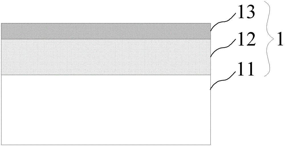
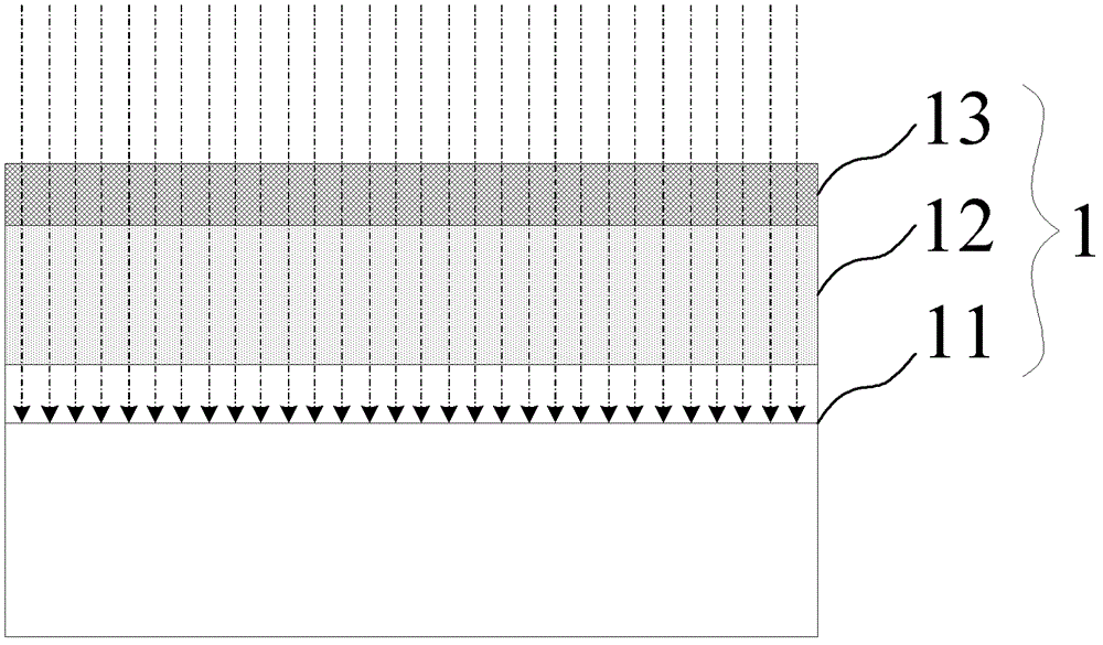
[0022] As shown in the figure, the present invention provides a method for preparing a tensile strained Ge thin film, at least comprising the following steps:

[0023] see figure 1 , providing a GaAs substrate 11 on which In x Ga 1-x As layer 12 and top Ge thin film 13, the In x Ga 1-x The In composition x in the As layer 12 is 0x Ga 1-x The thickness of the As layer 12 does not exceed the critical thickness of its growth on the GaAs substrate 11, so that the thickness of the top Ge film 13 does not exceed its growth on the In x Ga 1-x The critical thickness on the As layer 12 is used to prepare samples of Ge thin films. In this embodiment, In is epitaxially grown on the GaAs substrate 11 by molecular beam epitaxy (MBE) or metal organic compound chemical vapor deposition (MOCVD). x Ga 1-x As layer 12 and top Ge film 13; the In x Ga 1-x The thickness of the As layer is less than 1nm-1um. .


PUM

PropertyMeasurementUnit
Layer thicknessaaaaaaaaaa

Abstract

The invention provides a preparation method and laminated structure of a tensile strain Ge film. The preparation method includes the following steps: firstly, extending out an InxGa(1-x)As layer and a top layer Ge film on a GaAs underlayer, wherein the In component x is > 0 and <=1, the thickness of the InxGa(1-x)As layer is enabled to be no more than the critical thickness of the InxGa(1-x)As layer on the GaAs underlayer, and the thickness of the top layer Ge film is enabled to be no more than the thickness of the critical thickness of the top layer Ge film on the InxGa(1-x)As layer to prepare samples of the Ge film, secondly, infusing helium ions or hydrogen ions to the samples and enables peak values of the helium ions or the hydrogen ions to be distributed under a combined interface of the InxGa(1-x)As layer and the GaAs underlayer 10-100 nm, at last, conducting rapid thermal annealing to the samples to obtain relaxed InxGa(1-x)As layer and tensile strain Ge film. Thus purposes that Ge films with tensile strain and high migration rate are prepared with low cost, the thickness of a buffer layer of the InxGa(1-x)As is reduced, and penetrating dislocation density of the buffer layer of the InxGa(1-x)As is reduced.

Description

technical field [0001] The invention relates to the field of silicon-based optoelectronic integration, in particular to a preparation method and a stacked structure of a tensile strained Ge thin film. Background technique [0002] With the development of the information industry, information data will increase massively, and higher requirements and challenges will be put forward for the future development of information computing, transmission and other technologies. One of the main solutions is to combine the existing mature microelectronics and optoelectronics to realize silicon-based optoelectronic integration, which will become one of the important directions for the development of the information industry. In the past ten years, due to its great industrial significance, the research on key materials and devices for silicon-based optoelectronic integration has attracted serious attention from the international scientific community (such as MIT, Harvard University) and in...

Claims


Application Information

Patent Timeline
IPC IPC(8): H01L21/02H01L21/20
Inventor 张苗刘林杰狄增峰高晓强陈达薛忠营姜海涛卞建涛
Owner SHANGHAI INST OF MICROSYSTEM & INFORMATION TECH CHINESE ACAD OF SCI
Why Eureka
Try Eureka