Positive-negative-positive transistor integrated with germanium-silicon hetero-junction negative-positive-negative transistor

A PNP triode, triode technology, applied in the direction of transistors, electrical components, circuits, etc., can solve the problems that affect the production cost and yield of germanium-silicon heterojunction NPN triodes, influence, and the inability to realize the integration of PNP triodes, etc., so that the production cost will not be reduced Effect

Active Publication Date: 2015-04-08
SHANGHAI HUAHONG GRACE SEMICON MFG CORP
View PDF3 Cites 0 Cited by
  • Summary
  • Abstract
  • Description
  • Claims
  • Application Information

AI Technical Summary

Problems solved by technology

If the polysilicon in the emitter region 110 is etched first, and then the silicon germanium single crystal in the base region 111 and the silicon germanium polycrystal 108 are etched, the existing PNP triode integration cannot be realized.
Therefore, in order to realize the integration of the existing PNP transistor and the silicon-germanium heterojunction NPN transistor, it is necessary to change the manufacturing process of the existing germanium-silicon heterojunction NPN transistor, thereby affecting the production of the existing germanium-silicon heterojunction NPN transistor. , which affects the production cost and yield of the existing silicon-germanium heterojunction NPN transistor

Method used


Image

  • Positive-negative-positive transistor integrated with germanium-silicon hetero-junction negative-positive-negative transistor
  • Positive-negative-positive transistor integrated with germanium-silicon hetero-junction negative-positive-negative transistor
  • Positive-negative-positive transistor integrated with germanium-silicon hetero-junction negative-positive-negative transistor

Examples


Embodiment Construction

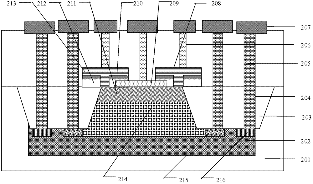
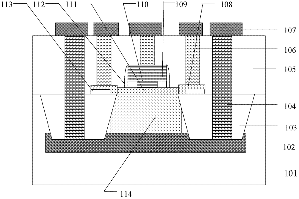
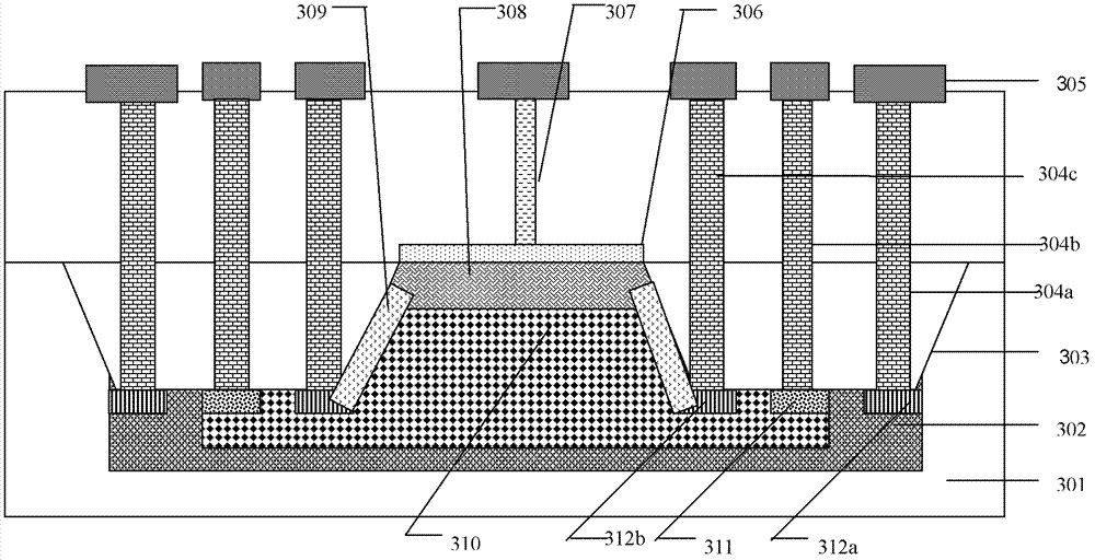
[0023] Such as image 3 Shown is a schematic structural diagram of a PNP transistor integrated with a germanium-silicon heterojunction NPN transistor according to an embodiment of the present invention. According to the embodiment of the present invention, the PNP transistor integrated with the germanium-silicon heterojunction NPN transistor is formed on a P-type substrate 301, and the active region is isolated by a shallow trench field oxygen 303, and an N-type deep NPN transistor is formed on the P-type substrate 301. Well 302, the PNP transistor is formed in the N-type deep well 302 and surrounded by the N-type deep well 302, a third deep hole contact 304a is formed in the shallow trench field oxygen 303, the third deep The N-type deep well 302 is led out by the hole contact 304 a , and an N-type buried layer 312 a is formed at the contact position between the third deep hole contact 304 a and the N-type deep well 302 . PNP transistors include:

[0024] The collector regi...


PUM


Abstract

The invention discloses a positive-negative-positive (PNP) transistor integrated with a germanium-silicon hetero-junction negative-positive-negative (NPN) transistor. A base area out-leading area is arranged on the lateral face of an active area to lead out a base area so that the fact that polycrystalline silicon is formed on the top portion of the active area to lead out the base area can be avoided, and therefore the integration of the PNP transistor and the germanium-silicon hetero-junction NPN transistor can be realized without changing the manufacturing process of the germanium-silicon hetero-junction NPN transistor, influences to the manufacturing of the germanium-silicon hetero-junction NPN transistor are prevented from being produced, and the facts that manufacturing cost of germanium-silicon hetero-junction NPN transistor is not increased and yield of the germanium-silicon hetero-junction NPN transistor is not reduced are guaranteed.

Description

technical field [0001] The invention relates to a semiconductor integrated circuit device, in particular to a PNP transistor integrated with a germanium-silicon heterojunction NPN transistor. Background technique [0002] For the Bipolar Field Effect Transistor (BiCMOS) process, as the complement of the NPN device, that is, the germanium-silicon heterojunction NPN transistor, the PNP device is also very important. PNP devices are generally divided into two types: lateral PNP and vertical PNP. Among them, the performance of the vertical PNP device is relatively high, which is also required in high-performance applications. However, the integration of vertical PNP devices and NPN devices is relatively difficult, or even impossible to integrate. The performance of the lateral PNP device is poor, but the integration of the device is relatively easy. [0003] Such as figure 1 As shown, it is a schematic structural diagram of an existing PNP transistor integrated with a german...

Claims


Application Information

Patent Timeline
Patent Type & Authority Patents(China)
IPC IPC(8): H01L29/73H01L29/06H01L29/10
Inventor 陈帆陈雄斌薛凯周克然潘嘉李昊王永成
Owner SHANGHAI HUAHONG GRACE SEMICON MFG CORP
Why Eureka
Try Eureka