
Silicon micro-flow-rate sensor chip in beam film single-beam structure

A flow sensor, single-beam structure technology, applied in the direction of volume/mass flow generated by electromagnetic effect, can solve the problems of difficult manufacturing process, long response time, compatibility, etc., and achieve the effect of small weight and small volume

Inactive Publication Date: 2013-05-01
XI AN JIAOTONG UNIV
View PDF3 Cites 5 Cited by
  • Summary
  • Abstract
  • Description
  • Claims
  • Application Information

AI Technical Summary

Problems solved by technology

However, thermal micro flow sensors also have their inherent disadvantages
For example, large power consumption, measurement error due to heat conduction of the substrate, zero point drift with ambient temperature, long response time, etc.
In addition, because of the need to heat the fluid, it limits the application of thermal micro-flow sensors in biotechnology
At present, there are relatively few studies on non-thermal flow sensors. The existing non-thermal flow sensors have problems such as difficulty in taking into account the sensitivity in the full range, generally difficult to calculate, and the manufacturing process is difficult to be compatible with standard CMOS processes.

Method used


Image

  • Silicon micro-flow-rate sensor chip in beam film single-beam structure
  • Silicon micro-flow-rate sensor chip in beam film single-beam structure
  • Silicon micro-flow-rate sensor chip in beam film single-beam structure

Examples


Embodiment Construction

[0016] The structure and working principle of the present invention will be described in detail below in conjunction with the accompanying drawings.

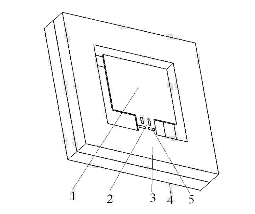
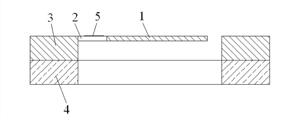
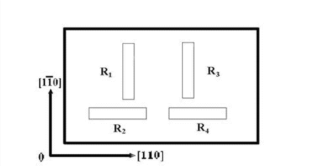
[0017] see figure 1 and figure 2 , a silicon micro-flow sensor chip with a beam film single beam structure, including a peripheral supporting silicon base 3, a glass substrate 4 is arranged on the back side of the peripheral supporting silicon base 3, and the back side of the peripheral supporting silicon base 3 is bonded to the glass substrate 4 The central silicon membrane 1 is located in the middle of the peripheral supporting silicon base 3, and one side of the central silicon membrane 1 and the peripheral supporting silicon base 3 are connected by a silicon cantilever beam 2, and the middle of the silicon cantilever beam 2 is equipped with four pressing Resistance strip 5, four piezoresistive strips 5 are connected to form a Wheatstone bridge, the beam-membrane structure composed of the central silicon membrane 1 and sili...


PUM


Abstract

The invention relates to a silicon micro-flow-rate sensor chip in a beam film single-beam structure. The silicon micro-flow-rate sensor chip comprises a peripheral support silicon base, wherein a glass substrate is arranged at the back side of the peripheral support silicon base, the back side of the peripheral support silicon base is in bonding connection with the glass substrate, a center silicon film is positioned in the middle of the peripheral support silicon base, one edge of the center silicon film is connected with the peripheral support silicon base through a silicon cantilever beam, the middle on the silicon cantilever arm is provided with four pressure resistance strips, the four pressure resistance strips are connected for forming a Whetstone electric bridge, a beam film structure formed by the center silicon film and the silicon cantilever beam forms a sensor measuring part, when fluid with certain speed acts on the sensor chip, the inertia force acts on the center silicon film, further, the beam film structure deforms, the resistance value of the pressure resistance strip is changed under the stress effect of the silicon cantilever beam, the Whetstone electric bridge is out of balance, and an electric signal corresponding to the external flow rate is output, so the measurement of the sensor chip on the flow rate is realized. The silicon micro-flow-rate sensor chip has the advantages that the size is small, the weight is light, the response speed is high, and the sensitivity is high.

Description

technical field [0001] The invention belongs to the technical field of micro-mechanical electronics, and in particular relates to a silicon micro-flow sensor chip with a beam-membrane single-beam structure. Background technique [0002] Flow measurement is an important detection parameter for industrial production and scientific research. In recent years, with the in-depth research and progress on micro-electro-mechanical systems (MEMS), traditional industrial and fluid mechanics research flow sensors are developing towards high integration, miniaturization, high precision, and high reliability. According to the measurement principle, MEMS flow sensors can be mainly divided into thermal type and non-thermal type. After 30 years of development, thermal MEMS flow sensors have occupied the mainstream position of flow measurement. However, thermal microflow sensors also have their inherent disadvantages. For example, large power consumption, measurement errors due to thermal c...

Claims


Application Information

Patent Timeline
IPC IPC(8): G01F1/56
Inventor 赵玉龙陈佩李一瑶
Owner XI AN JIAOTONG UNIV
Learn More