Method For Solidifying A Semiconductor With Adding Charges Of A Doped Semiconductor During The Crystallisation

A curing method and semiconductor technology, applied in semiconductor devices, chemical instruments and methods, crystal growth, etc., can solve problems such as non-uniform resistivity, resistivity reduction, and severe

Inactive Publication Date: 2013-05-08
COMMISSARIAT A LENERGIE ATOMIQUE ET AUX ENERGIES ALTERNATIVES
View PDF8 Cites 11 Cited by
  • Summary
  • Abstract
  • Description
  • Claims
  • Application Information

AI Technical Summary

Problems solved by technology

And if the silicon contains a lot of phosphorous for a given resistivity, the effect will be even more dramatic
[0016] This change in conductivity type was not observed in the n-type ingot, since the concentration of phosphorous was always maintained higher than that of boron, however the difference between these concentrations was greater at the top of the ingot than will be larger from the beginning of the ingot, thus resulting in a non-uniform resistivity that decreases along the height of the ingot
[0017] Therefore, in all cases, most of the ingots were not suitable for use, either because of inhomogeneity in resistivity or because of variations in conductivity type

Method used


Image

  • Method For Solidifying A Semiconductor With Adding Charges Of A Doped Semiconductor During The Crystallisation
  • Method For Solidifying A Semiconductor With Adding Charges Of A Doped Semiconductor During The Crystallisation
  • Method For Solidifying A Semiconductor With Adding Charges Of A Doped Semiconductor During The Crystallisation

Examples


Embodiment Construction

[0075] Below in conjunction with specific embodiment, further set forth the present invention:

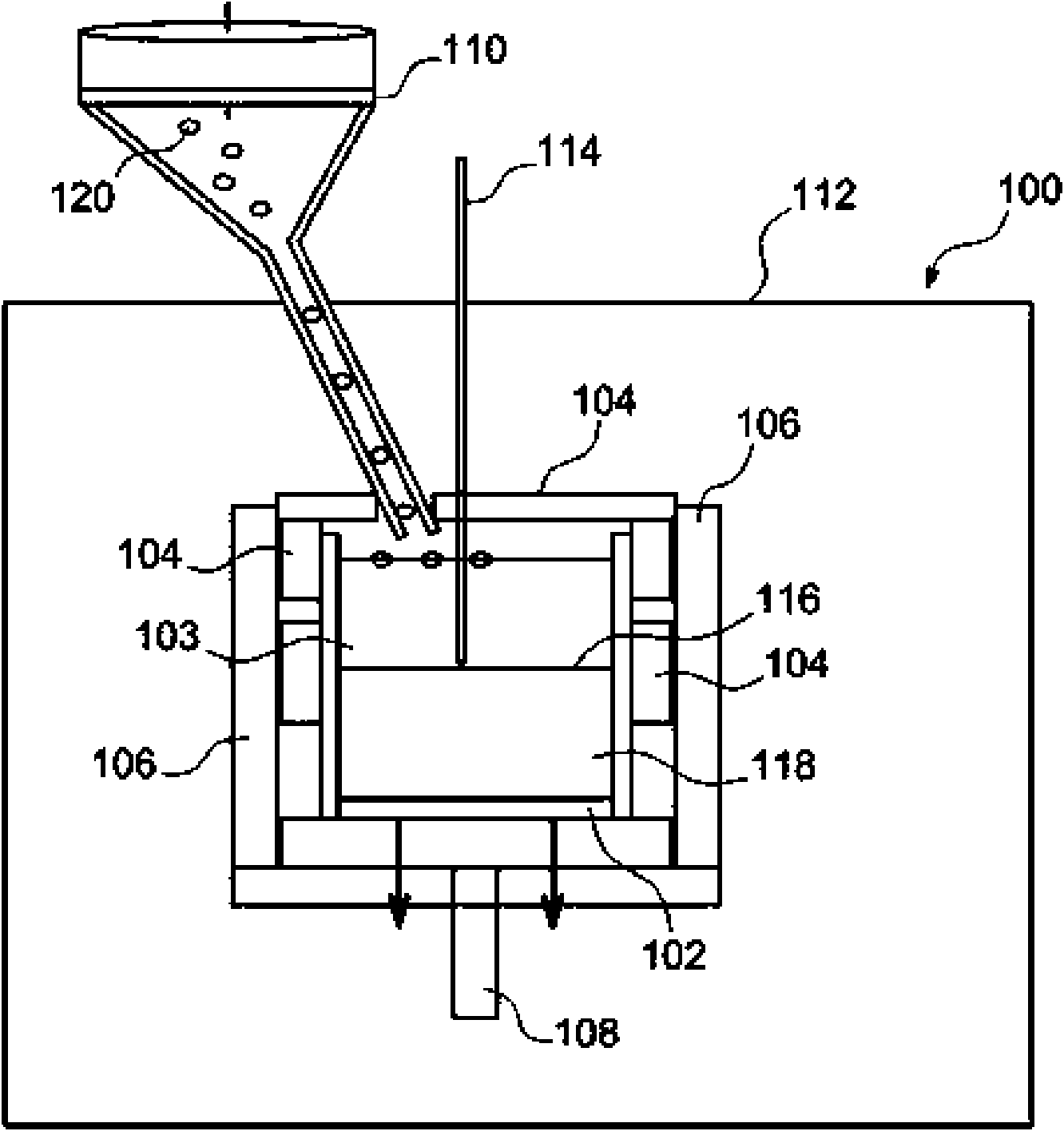
[0076] Such as figure 1 As shown, the figure shows a crystal growth Bridgman drop furnace 100, or zone melting oven, in which a semiconductor solidification process, in this example a crystallization operation, is performed.

[0077] The oven 100 includes a crucible 102 designed to hold molten semiconductor 103 to be crystallized. exist figure 1 In this crucible 102 a crystallized semiconductor 118 is obtained, ie located below the immersion bath in which the semiconductor 103 is melted. The oven 100 also contains heating means 104 , which are, for example electrically supplied, arranged above the crucible 102 and rest at the upper part of the side walls of the crucible 102 . The heating elements 104 are used to melt the semiconductor as it is introduced into the crucible 102 in solid form and maintain it in a molten form. The oven 100 also includes an insulated side wall 106 ....


PUM


Abstract

A method for semiconductor solidification which includes steps for: forming a bath of molten semiconductor from a first charge of semiconductor which includes dopants, solidification of the molten semiconductor, and which in addition includes, during solidification, the implementation of one or more steps for the addition of supplementary charges of semiconductor, which also contains dopants, to the molten semiconductor bath. The method has homogeneous resistivity throughout the solidified semiconductor, whilst preventing changes in the type of conductivity over the entire or a very large part of the semiconductor and which does not adversely effect the electrical properties of devices made from the semiconductor that is obtained.

Description

technical field [0001] The present invention relates to a silicon semiconductor solidification method, more specifically, it is a semiconductor solidification method that adds dopant semiconductor feedstock in the crystallization process, which can remove the semiconductor dopant in the semiconductor solidification process Processing is controlled. The invention is particularly applicable to the crystallization of liquid metallurgical silicon in the form of ingots or ribbons for the manufacture of photovoltaic cell substrates. Background technique [0002] During the directional solidification of a semiconductor containing one or more dopants, the dopant concentration changes along the direction of crystallization because the composition of the formed solid is different from that of the liquid (at large Dopant accumulation usually occurs in this liquid in most general cases). In more detail, with the liquid fully mixed, the dopant distribution in the ingot along the direct...

Claims


Application Information

Patent Timeline
Patent Type & Authority Applications(China)
IPC IPC(8): C30B15/04C30B11/04C30B13/10C30B29/06H01L31/18
CPCC30B11/04C30B29/06C30B15/04C30B13/10
Inventor 斯万特˙佛罗伦萨卡梅尔˙丹尼斯
Owner COMMISSARIAT A LENERGIE ATOMIQUE ET AUX ENERGIES ALTERNATIVES
Why Eureka
Try Eureka