Vertical double-diffused metal oxide semiconductor field effect transistor having semi-insulating polysilicon layer

A technology of semi-insulating polysilicon and oxide semiconductors, which is applied in semiconductor devices, semiconductor/solid-state device manufacturing, electrical components, etc., and can solve the problems of increased conduction loss of devices

Active Publication Date: 2017-08-15
XIDIAN UNIV
View PDF2 Cites 4 Cited by
  • Summary
  • Abstract
  • Description
  • Claims
  • Application Information

AI Technical Summary

Problems solved by technology

However, in the field of high-voltage applications of power devices, as the breakdown voltage of the device increases, the thickness of the power VDMOS epitaxial layer increases continuously, and the doping concentration of the drift region gradually decreases, resulting in the on-resistance of the device decreasing with 2.5% of the breakdown voltage of the device. time increases sharply, which increases the conduction loss of the device

Method used


Image

  • Vertical double-diffused metal oxide semiconductor field effect transistor having semi-insulating polysilicon layer

Examples


Embodiment Construction

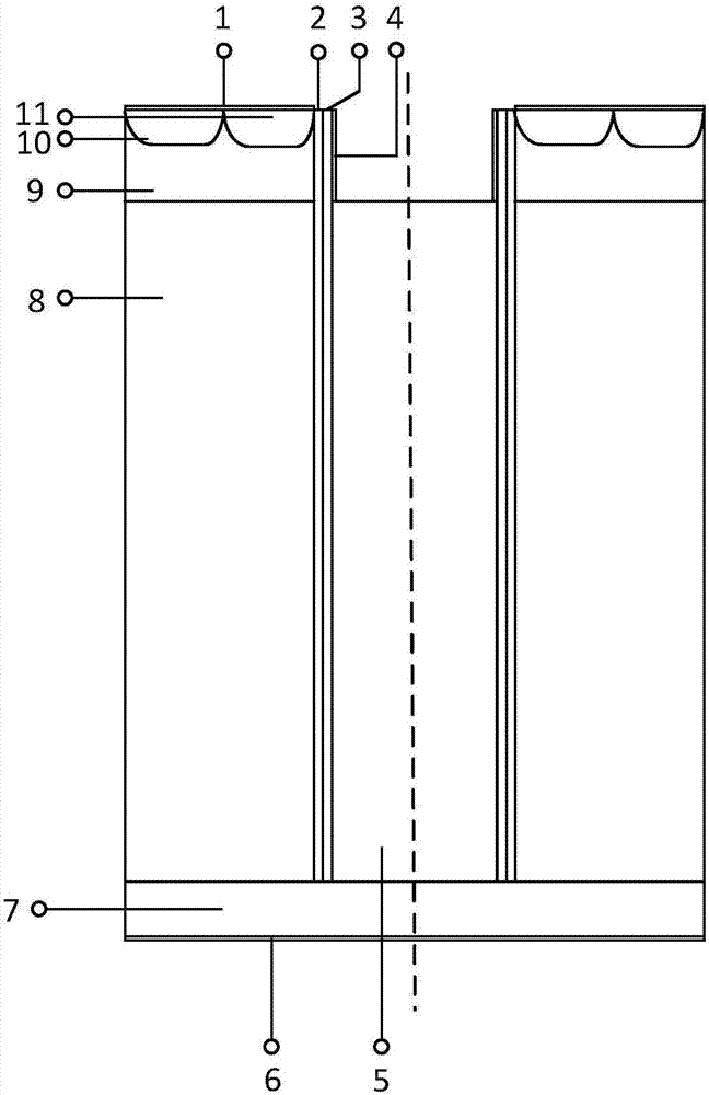
[0044] Such as figure 1 As shown, the vertical double-diffused metal oxide semiconductor field effect transistor with a semi-insulating polysilicon layer includes:

[0045] Substrate drain region 7 of semiconductor material with a doping concentration of 1×10 13 cm -3 ~1×10 15 cm -3 ;

[0046] A drift region 8 formed by an epitaxial layer on the substrate;

[0047] a base region 9 formed by doping on the drift region;

[0048] Etching a trench on the base region, the trench goes down through the drift region to the substrate drain region;

[0049] The gate insulating layer 2 formed on the side wall of the trench has a thickness of 0.02-0.1 μm;

[0050] Oxygen-doped semi-insulating polysilicon layer 3 deposited outside the gate insulating layer; the thickness of the semi-insulating polysilicon layer is 0.2-1.5 μm; the oxygen-doped ratio of the semi-insulating polysilicon layer is 15%-35%, and its corresponding resistivity for 10 9 ~10 11 Ω cm;

[0051] Depositing an ...


PUM


Abstract

The invention provides a vertical double-diffused metal oxide semiconductor field effect transistor (VDMOS) having a semi-insulating polysilicon layer (SIPOS). The VDMOS is mainly characterized in that an SIPOS filling layer is formed on the side wall of a device drift region, and two ends of the SIPOS filling layer are connected with a gate end and a drain end of the VDMOS. On one hand, since the SIPOS has uniform resistivity, the SIPOS has a uniform electric field when the VDMOS is turned off. According to an electric displacement continuity equation, an electric field on the device drift region is modulated by means of the uniform electric field on the SIPOS and becomes more uniform, and the SIPOS layer enhances the depletion of the device drift region of the VDMOS, thus doping concentration of the device drift region is increased, and the VDMOS has low on-resistance when being turned on; on the other hand, since a potential difference exists between the surfaces of the SIPOS layer and the device drift region, the device drift region has majority carrier accumulation, thereby further decreasing the on-resistance of the VDMOS.

Description

technical field [0001] The invention relates to the field of semiconductor devices, in particular to a trench (Trench) type vertical double-diffused metal oxide semiconductor field effect transistor. Background technique [0002] The development of power semiconductor devices has brought electronic products into a new stage. Power MOSFET is a multi-subconductive device, which has the advantages of fast switching speed, high input impedance, easy driving, and no secondary breakdown phenomenon. In 1985, a trench (Trench) MOS structure was proposed by D.Ueda et al. The U-shaped groove structure makes the conduction channel of the device change from horizontal to vertical, which effectively eliminates the resistance of JFET, greatly increases the original cell density, and improves the current handling capacity of the device. However, in the field of high-voltage applications of power devices, as the breakdown voltage of the device increases, the thickness of the power VDMOS e...

Claims


Application Information

Patent Timeline
Patent Type & Authority Applications(China)
IPC IPC(8): H01L29/78H01L29/06H01L21/336
CPCH01L29/0611H01L29/0684H01L29/66712H01L29/7802
Inventor 段宝兴曹震师通通吕建梅袁嵩杨银堂
Owner XIDIAN UNIV
Why Eureka
Try Eureka