
A high power thyristor

A thyristor and high-power technology, applied in the field of power switching devices, can solve the problems of reduced on-state average current density, poor distribution uniformity of on-state current density, and prolonged turn-on time, achieving high on-state average current density and high current Uniform density distribution and low on-state power consumption

Active Publication Date: 2015-09-16
HANGZHOU HANAN SEMICON
View PDF4 Cites 2 Cited by
  • Summary
  • Abstract
  • Description
  • Claims
  • Application Information

AI Technical Summary

Problems solved by technology

However, as the diameter of the silicon chip continues to increase with the increase of power, the length of the amplification gate will inevitably increase, and its parasitic distributed resistance and capacitance will increase rapidly.
Due to the above reasons, the size of the gate of the unit cell structure increases, which is affected by the increase of the parasitic resistance and capacitance of the central gate and the amplified gate, which increases the charging time constant of the thyristor during the turn-on process, causing the turn-on time to be prolonged and the turn-on speed to slow down. , the di / dt tolerance of the opening process is reduced, and the opening uniformity is deteriorated; at the same time, the uniformity of the on-state current density distribution is deteriorated, the effective on-state average current density is reduced, and the on-state voltage drop and on-state power consumption are increased.

Method used


Image

  • A high power thyristor
  • A high power thyristor
  • A high power thyristor

Examples


Embodiment Construction

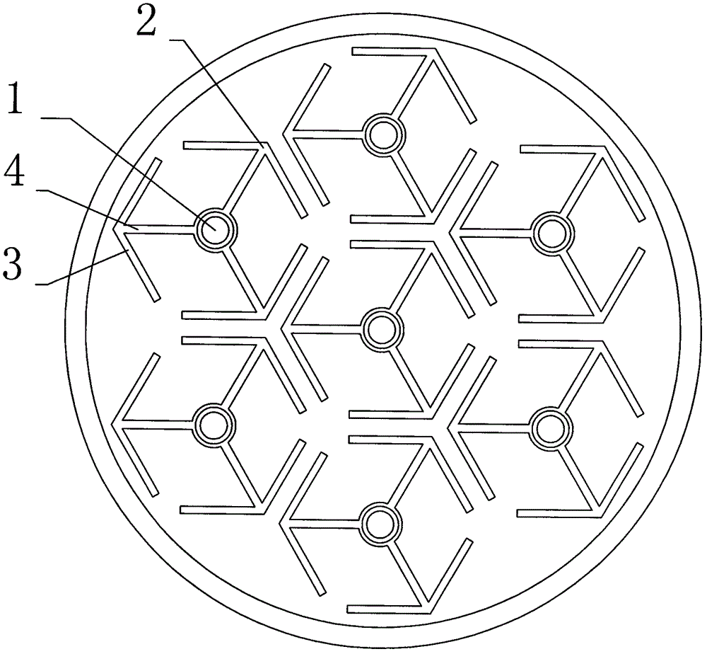
[0011] The high-power thyristor of the first embodiment of the present invention is provided with a silicon wafer, and seven unit cell gates with the same structure are provided on the silicon wafer. Such as figure 1 As shown, each cell gate is composed of a central gate 1 and an enlarged gate 2. The enlarged gate 2 includes three arrow-shaped fingers. Each finger is provided with a flange part 3 that is bent 120 degrees. The center gate electrode is in the middle of the flange part 3, that is, at the junction of the two sides. A connecting part 4 is provided in the direction of 1. The sub-fingers are distributed around the central gate 1 in a circle with an interval of one hundred and two degrees. The connecting parts 4 of the three sub-fingers are interwoven and connected around the central gate 1, and then the connecting parts 4 of the sub-fingers are in a radius centered on the central gate 1 In the direction, the folded edges 3 of adjacent finger points are separated.

[0...


PUM


Abstract

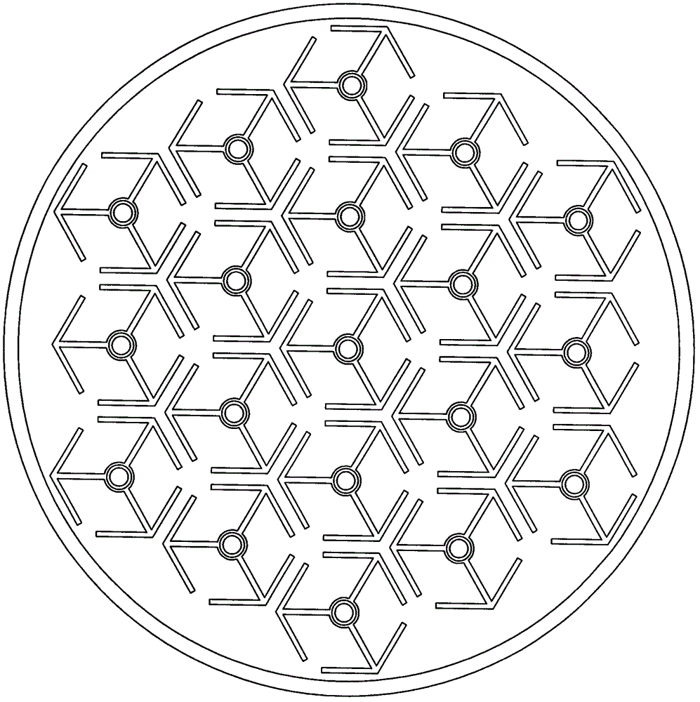
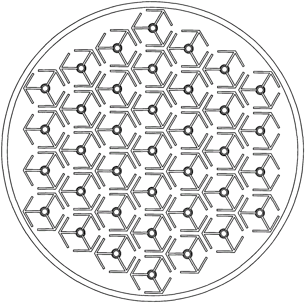
The invention discloses a high-power thyristor which comprises a silicon wafer, the silicon wafer is provided with unit cell gate poles, each unit cell gate pole comprises a central gate pole and an amplification gate pole, each central gate pole is located at the dead center of each amplification gate pole, the silicon wafer is provided with at least seven unit cell gate poles, and any three adjacent unit cell gate poles are distributed on the silicon wafer in a regular triangle shape. A plurality of small-size unit cell gate poles are installed on the silicon wafer of the high-power thyristor, multiple-unit cell structure gate poles are formed on the surface of the silicon wafer of the high-power thyristor, a plurality of parasitic resistors and a plurality of working areas which are small in capacitance are built on the surface of the silicon wafer, so that the thyristor which is large in size has the same working properties with a thyristor which is small in size, and the high-power thyristor has the advantages of being high in starting speed, even in current density distribution, high in on-state average current density, low in on-state voltage-drop, and low in on-state power consumption. Therefore, by means of the technical scheme, switching operation which is good in performance can be achieved on the high-power thyristor which is larger in size.

Description

Technical field [0001] The invention relates to a power switch device, in particular to a high-power thyristor. Background technique [0002] A silicon chip is arranged in the thyristor, and the silicon chip is circular. The gate electrode with the unit cell structure is provided on the silicon wafer, that is, only a central gate electrode and an enlarged gate electrode surrounding the central gate electrode are provided on the silicon wafer. The magnification gate usually adopts a mushroom-shaped multi-finger structure or an involute multi-finger structure to cover the silicon chip. However, as the diameter of the silicon wafer continues to increase with the increase of power, the length of the amplification gate inevitably increases, and its parasitic distributed resistance and capacitance increase rapidly. Due to the above reasons, the size of the gate of the unit cell structure increases, which is affected by the parasitic resistance and capacitance increase of the central ...

Claims


Application Information

Patent Timeline
Patent Type & Authority Patents(China)
IPC IPC(8): H01L29/74H01L29/423
CPCH01L29/0692H01L29/42308H01L29/74
Inventor 王勇张海鹏
Owner HANGZHOU HANAN SEMICON
Learn More