Light-emitting diode (LED) lighting structure

A light-emitting structure, quantum well technology, applied in electrical components, circuits, semiconductor devices, etc., can solve the problems of low carrier recombination efficiency, lattice mismatch, weak two-dimensional confinement of electron holes, etc., to improve the recombination efficiency. , The effect of reducing internal stress and improving lattice matching rate

Active Publication Date: 2013-05-22
广东昭信集团股份有限公司
View PDF3 Cites 8 Cited by
  • Summary
  • Abstract
  • Description
  • Claims
  • Application Information

AI Technical Summary

Problems solved by technology

[0004] In the technical solution provided by the Chinese invention patent with the application number 200910046837.9, the above factors also exist, and since the application uses a ternary InGaN / GaN quantum well structure, the InGaN of the first and second quantum wells The lattice mismatch between the well layer and the (In)GaN barrier layer; in addition, the two-dimensional confinement of electrons and holes generated by the InGaN well layer and the (In)GaN barrier layer of the first and second types of quantum wells is weak, and the current-carrying The recombination efficiency of electrons in the quantum well is low

Method used


Image

  • Light-emitting diode (LED) lighting structure
  • Light-emitting diode (LED) lighting structure
  • Light-emitting diode (LED) lighting structure

Examples


Embodiment Construction

[0015] An LED lighting structure provided by the present invention will be described in detail below with reference to the accompanying drawings and specific embodiments.

[0016] In the following description, various aspects of the present invention will be described. However, those skilled in the art can implement the present invention by using only some or all of the structures or processes of the present invention. For clarity of explanation, specific numbers, arrangements and sequences are set forth, but it will be apparent that the invention may be practiced without these specific details. In other instances, well-known features have not been described in detail in order not to obscure the invention.

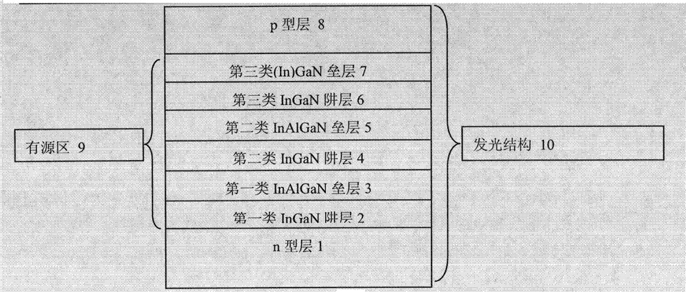
[0017] In general, the present application provides a long-wavelength LED light-emitting structure, which adopts the form of three kinds of quantum wells containing different components of indium and / or aluminum. Depending on the application, they can be designed to emit ...


PUM


Abstract

The invention provides a light-emitting diode (LED) lighting structure. The LED lighting structure comprises a p type doped region, a n-type doped region and a lighting active region, wherein the p-type doped region is used for injecting into a hole, the n-type doped region is located on the bottom and used for injecting electrons and the lighting active region is located on the n-type doped region. The LED lighting structure is characterized in that the lighting active region comprises at least one InGaN trap layer and at least one InAlGaN barrier layer of a first type quantum well, at least one InGaN trap layer and at least one InAlGaN barrier layer of a second type quantum well and at least one InGaN trap layer and at least one InAlGaN barrier layer of a third type quantum well.

Description

technical field [0001] The invention relates to a light-emitting structure, which includes an LED light-emitting structure of indium-aluminum-gallium-nitride quantum well. Background technique [0002] At present, LEDs with InGaN well layers containing indium-gallium-nitride quantum wells are attracting more and more attention from the industry, but the InGaN base of this type of LEDs is in the market for high luminous efficiency, long wavelength (green light) and high indium components. There is no perfect solution yet. In traditional light-emitting structures, there are usually huge internal stress problems. [0003] The lattice mismatch between InGaN and GaN is the reason why the high indium composition InGaN quantum wells are difficult to grow. The InGaN well layer and GaN barrier layer containing high indium composition will generate large internal stress, thereby generating dislocations in the quantum well. It is well known that dislocations are the main cause of no...

Claims


Application Information

Patent Timeline
Patent Type & Authority Applications(China)
IPC IPC(8): H01L33/06
Inventor 方方
Owner 广东昭信集团股份有限公司
Why Eureka
Try Eureka