A parasitic n-i-p type pin device structure and manufacturing method in a bicmos process

An N-I-P, device structure technology, applied in semiconductor/solid-state device manufacturing, semiconductor devices, electrical components, etc., can solve problems such as large insertion loss and limited forward conduction current capability

Active Publication Date: 2016-04-13
SHANGHAI HUAHONG GRACE SEMICON MFG CORP
View PDF5 Cites 0 Cited by
  • Summary
  • Abstract
  • Description
  • Claims
  • Application Information

AI Technical Summary

Problems solved by technology

like figure 1 As shown, the disadvantage of a traditional PIN device structure is that the forward current capability is limited and the insertion loss is large.

Method used


Image

  • A parasitic n-i-p type pin device structure and manufacturing method in a bicmos process
  • A parasitic n-i-p type pin device structure and manufacturing method in a bicmos process
  • A parasitic n-i-p type pin device structure and manufacturing method in a bicmos process

Examples


Embodiment Construction

[0025] Such as figure 2 Shown, the parasitic N-I-P type PIN device structure of the present invention comprises:

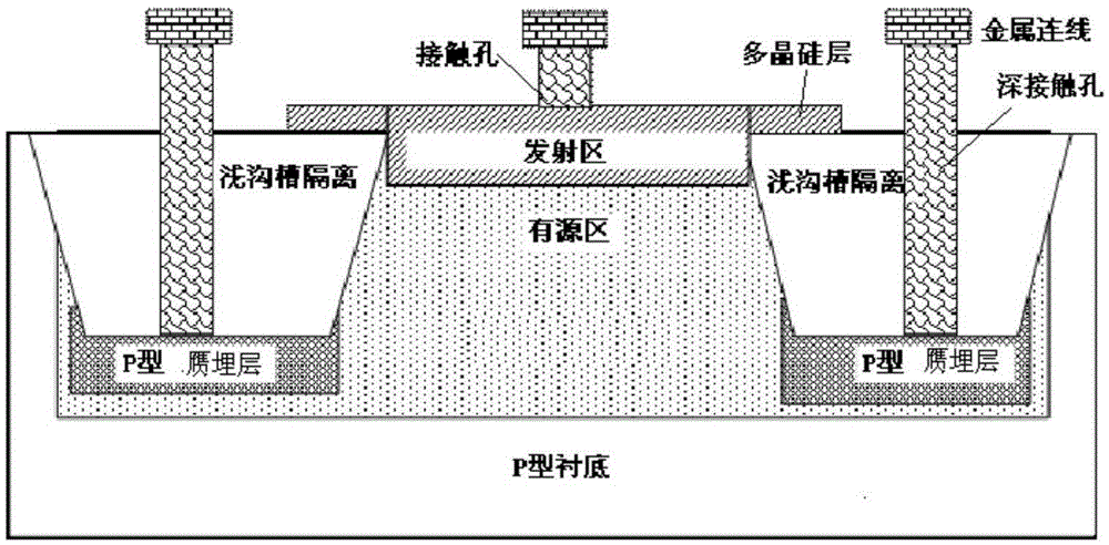
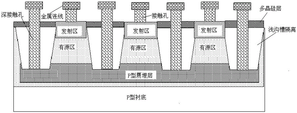
[0026] An active region is formed above the P-type substrate, and a P-type pseudo-buried layer is formed in the active region. A plurality of shallow trench isolations are formed above the P-type pseudo-buried layer, and a polysilicon layer is formed on the shallow trench isolation. An emitter region is formed above the source region, and the emitter region and the polysilicon layer are alternately arranged. The emitter region is connected to a metal wire through a contact hole, and the P-type pseudo-buried layer is connected to a metal wire through a deep contact hole. The deep contact hole has titanium or tin and tungsten.

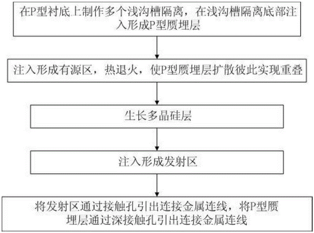
[0027] Such as image 3 Shown, the manufacturing method of parasitic N-I-P type PIN device structure of the present invention comprises:

[0028] (1) if Figure 4 As shown, a plurality of shallow trench isolations are made on a P-type s...


PUM


Abstract

The invention discloses a parasitic N-I-P type PIN device structure in a BiCMOS (bipolar complementary metal oxide semiconductor) process. The parasitic N-I-P type PIN device structure is characterized in that an active area is formed above a P type substrate, a P type embedded layer is formed in the active area, a plurality of shallow trench isolators are formed above the P type embedded layer, polycrystalline silicon layers are formed above the shallow trench isolators, emitting areas are formed above the active area, the emitting areas and the polycrystalline silicon layers are alternately arranged, the emitting areas are connected with metal wires in a leading-out manner through contact holes, the P type embedded layer is connected with a metal wire in a leading-out manner through a deep contact hole, and titanium or tin and tungsten are arranged in the deep contact hole. The invention further discloses a manufacturing method of the parasitic N-I-P type PIN device structure in the BiCMOS process. By the aid of the parasitic N-I-P type PIN device structure and the manufacturing method thereof, forward breakover current and the effective area of a PIN device can be increased, and insertion loss of the PIN device is reduced.

Description

technical field [0001] The invention relates to the field of semiconductor manufacturing, in particular to a parasitic N-I-P type PIN device structure in a BiCMOS process. The invention also relates to a manufacturing method of a parasitic N-I-P type PIN device structure in a BiCMOS process. Background technique [0002] The conventional Bipolar (insulated gate bipolar transistor) uses a highly doped buried layer in the collector area to reduce the resistance of the collector area, and uses high-concentration and high-energy N-type implantation to connect the buried layer in the collector area to form a collector terminal. (collector pick-up). The low-medium doped collector region is epitaxy on the buried layer of the collector region, the base region is formed on the P-type doped epitaxy, and then the heavily N-type doped polysilicon forms the emitter, and finally the bipolar is completed. Such as figure 1 As shown, the disadvantage of a traditional PIN device structure ...

Claims


Application Information

Patent Timeline
Patent Type & Authority Patents(China)
IPC IPC(8): H01L29/73H01L29/06H01L21/331
Inventor 胡君刘冬华钱文生段文婷石晶
Owner SHANGHAI HUAHONG GRACE SEMICON MFG CORP
Why Eureka
Try Eureka