

PIN device in bipolar complementary metal oxide semiconductor (BiCMOS) process
A device and process technology, applied in the field of semiconductor integrated circuit devices, can solve the problems of uneven forward conductor current and large series resistance, and achieve the effects of uniform current, improved characteristics and reduced series resistance
- Summary
- Abstract
- Description
- Claims
- Application Information
AI Technical Summary
Problems solved by technology
Method used
Image

Examples
Embodiment B
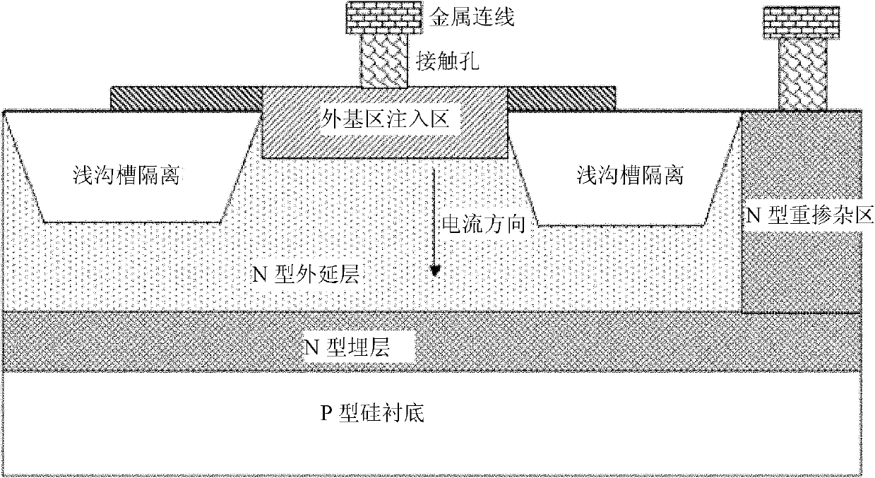
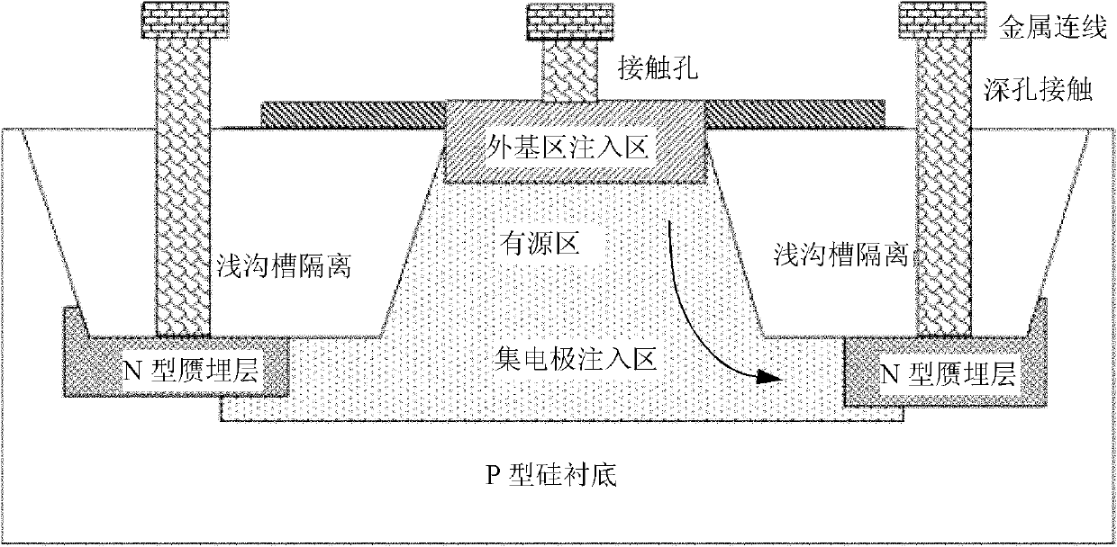
[0017] Such as Figure 4 Shown is a schematic diagram of the structure of the top view of the PIN device of the embodiment of the present invention; Figure 5E The above is a schematic diagram of a cross-sectional structure of a PIN device according to an embodiment of the present invention. The PIN device in the BiCMOS process of the embodiment of the present invention is formed on a P-type silicon substrate, and the active region is isolated by shallow trench field oxygen.
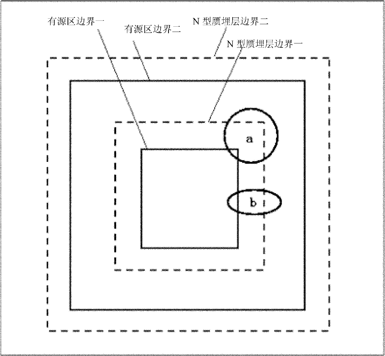
[0018] Such as Figure 4 As shown, in a plan view, the layout structure of the PIN device according to the embodiment of the present invention is an octagon. Among them, the active region boundary 1, the active region boundary 2, the N-type pseudo-buried layer boundary 1, and the N-type pseudo-buried layer boundary 2 are all octagonal. The inner region of the boundary of the active region is the region where the active region is formed, and the region between the boundary of the active region and the ...
PUM
 Abstract
Description
Claims
Application Information