Directionally recrystallized graphene growth substrates

A technology for recrystallization, graphene, applied in graphene, nanotechnology for materials and surface science, coatings, etc.

Inactive Publication Date: 2013-05-29
EMPIRE TECH DEV LLC
View PDF4 Cites 7 Cited by
  • Summary
  • Abstract
  • Description
  • Claims
  • Application Information

AI Technical Summary

Problems solved by technology

However, defects in graphene production, such as nucleation of multilayer graphene, can occur at metal grain boundaries in the growing layers of the graphene substrate

Method used


Image

  • Directionally recrystallized graphene growth substrates
  • Directionally recrystallized graphene growth substrates
  • Directionally recrystallized graphene growth substrates

Examples


Embodiment Construction

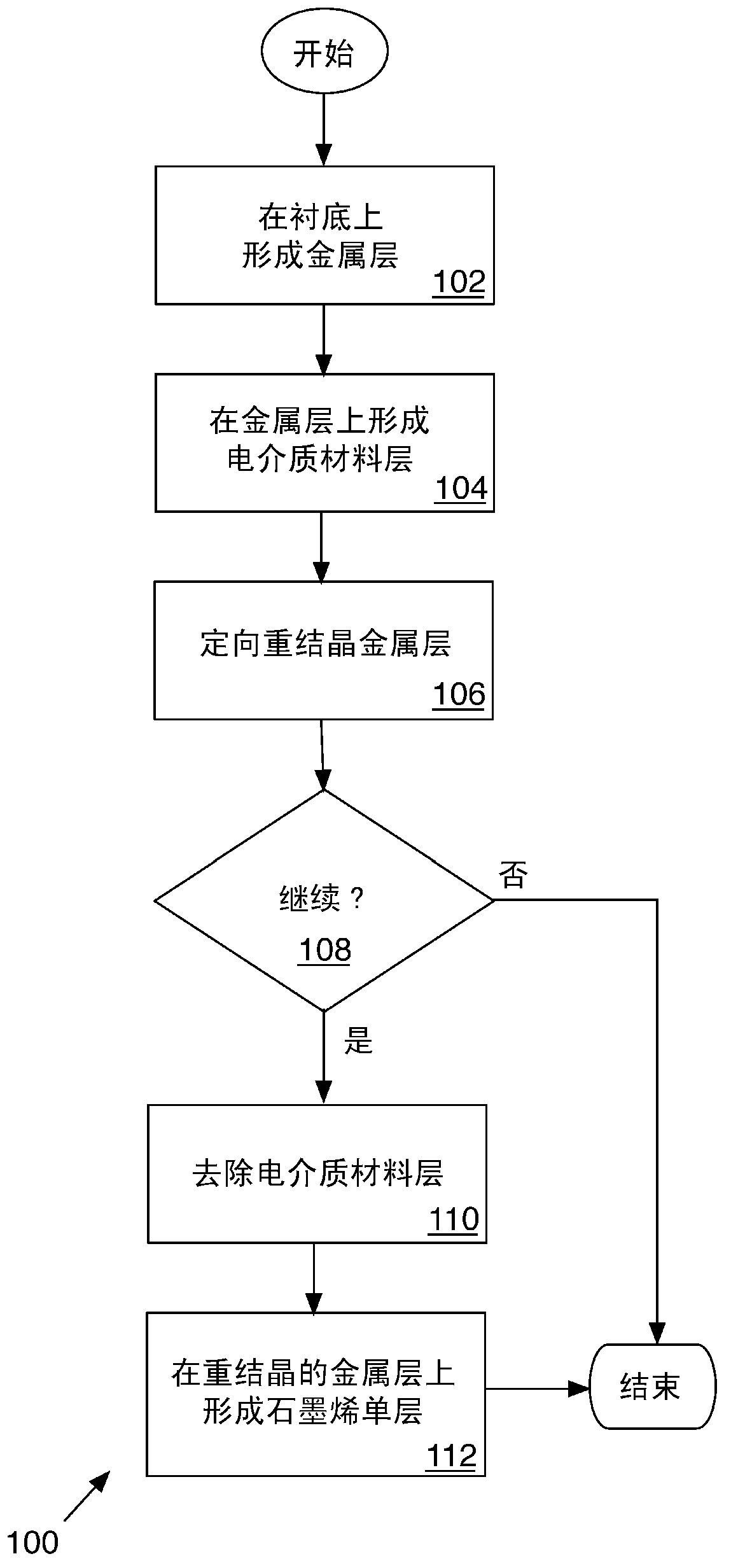
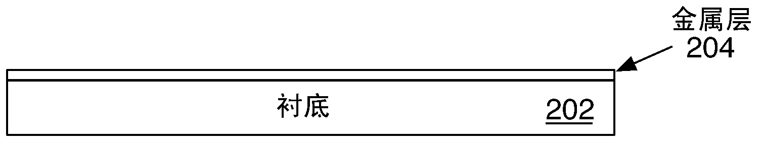
[0016] The following description sets forth various examples with specific details in order to provide a thorough understanding of claimed subject matter. It will be understood, however, to one of ordinary skill in the art, that claimed subject matter may be practiced without some or more of the specific details disclosed herein. Additionally, in some instances, well-known methods, procedures, systems, components and / or circuits have not been described in detail to avoid unnecessarily obscuring claimed subject matter. In the following detailed description, reference is made to the accompanying drawings which form a part hereof. In the drawings, similar symbols typically identify similar components, unless context dictates otherwise. The exemplary embodiments described in the detailed description, drawings, and claims are not limiting. Other embodiments may be utilized, and other changes may be made, without departing from the spirit or scope of the subject matter presented h...


PUM


Abstract

Implementations and techniques for producing substrates suitable for growing graphene monolayers are generally disclosed.

Description

Background technique [0001] Unless otherwise indicated, the materials described in this section are not prior art to the claims in this application and are not admitted to be prior art by inclusion in this section. [0002] Graphene, typically a planar single-layer array of carbon atoms, can be grown using chemical vapor deposition (CVD) on a substrate surface coated with a layer of nickel (Ni), ruthenium (Ru), or copper (Cu). However, defects in graphene production, such as nucleation of multilayer graphene, may occur at metal grain boundaries in the growing layers of the graphene substrate. Controlling the morphology of the growth layer by limiting the number of metal grain boundaries can improve the morphology of the graphene film, which in turn can improve the occurrence of production defects such as multilayer graphene. [0003] Directional crystallization (also known as excimer laser annealing) has been used to control the morphology of silicon (Si) layers in active mat...

Claims


Application Information

Patent Timeline
IPC IPC(8): C01B31/02C03B29/00C23C16/26H01L21/20
CPCC23C16/0281C01B31/0453C01B2204/32C23C16/52H01L21/02491H01L21/02658H01L21/02527C23C16/26B82Y30/00B82Y40/00C01B32/186
Inventor 托马斯·A·叶戈
Owner EMPIRE TECH DEV LLC
Why Eureka
Try Eureka