Method of manufacturing field termination type insulated gate bipolar translator (IGBT) component with substrate provided with outward-extending layer

A technology of epitaxial layer and manufacturing field, which is applied in the field of IGBT device manufacturing, can solve the problems of broken, large silicon wafers, increased costs, etc., and achieve the effect of reducing the chance of fragmentation and saving huge costs

Active Publication Date: 2013-06-05
SHANGHAI HUAHONG GRACE SEMICON MFG CORP
View PDF4 Cites 6 Cited by
  • Summary
  • Abstract
  • Description
  • Claims
  • Application Information

AI Technical Summary

Problems solved by technology

[0011] The general-purpose equipment of semiconductor manufacturers is used to process silicon wafers with a standard thickness (generally 725 μm), and there is a greater risk of silicon wafer breakage when handling extremely thin slices
And repurchasing equipment that can handle extremely thin sheets will greatly increase the cost and affect the overall production capacity

Method used


Image

  • Method of manufacturing field termination type insulated gate bipolar translator (IGBT) component with substrate provided with outward-extending layer
  • Method of manufacturing field termination type insulated gate bipolar translator (IGBT) component with substrate provided with outward-extending layer
  • Method of manufacturing field termination type insulated gate bipolar translator (IGBT) component with substrate provided with outward-extending layer

Examples


Embodiment Construction

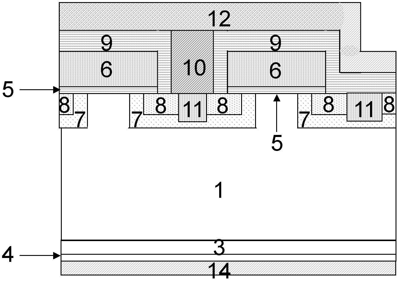
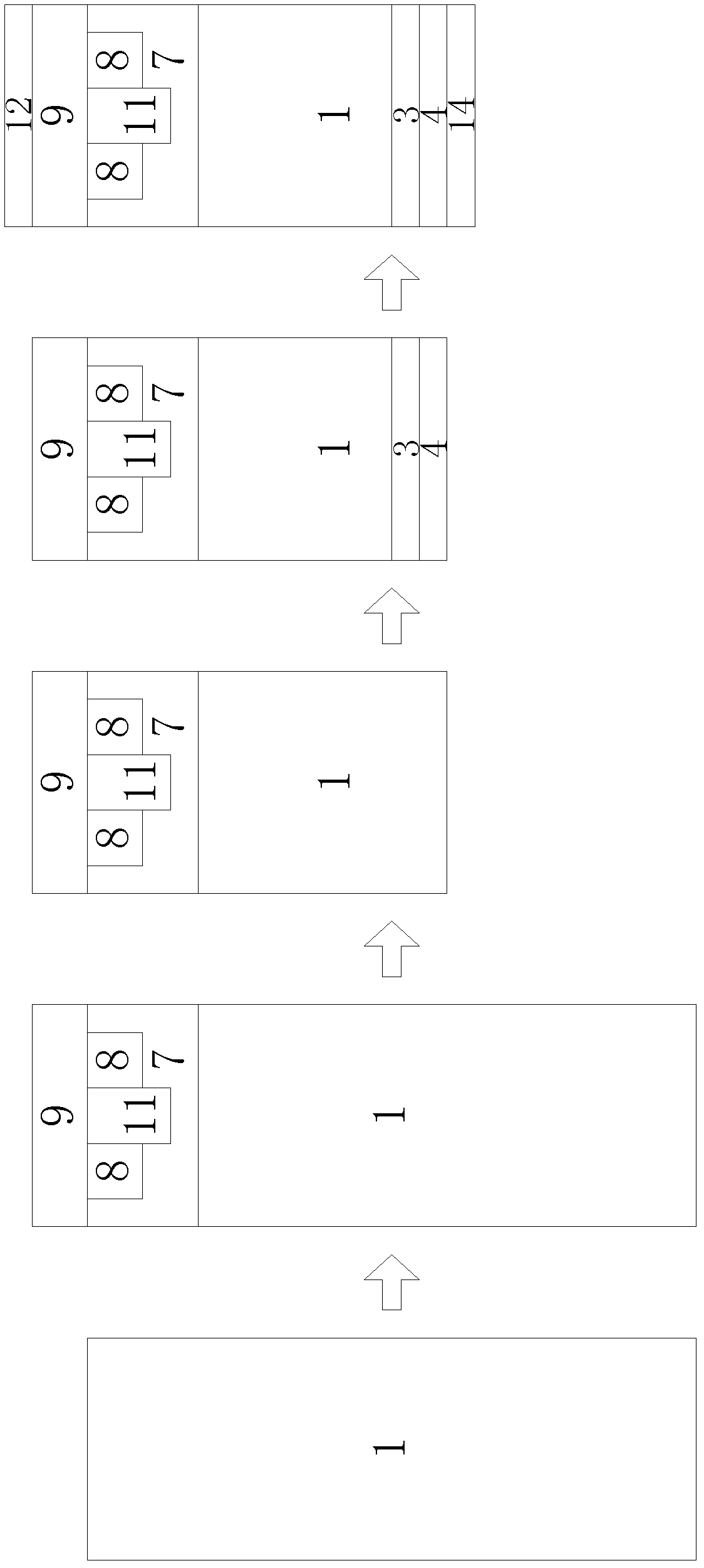
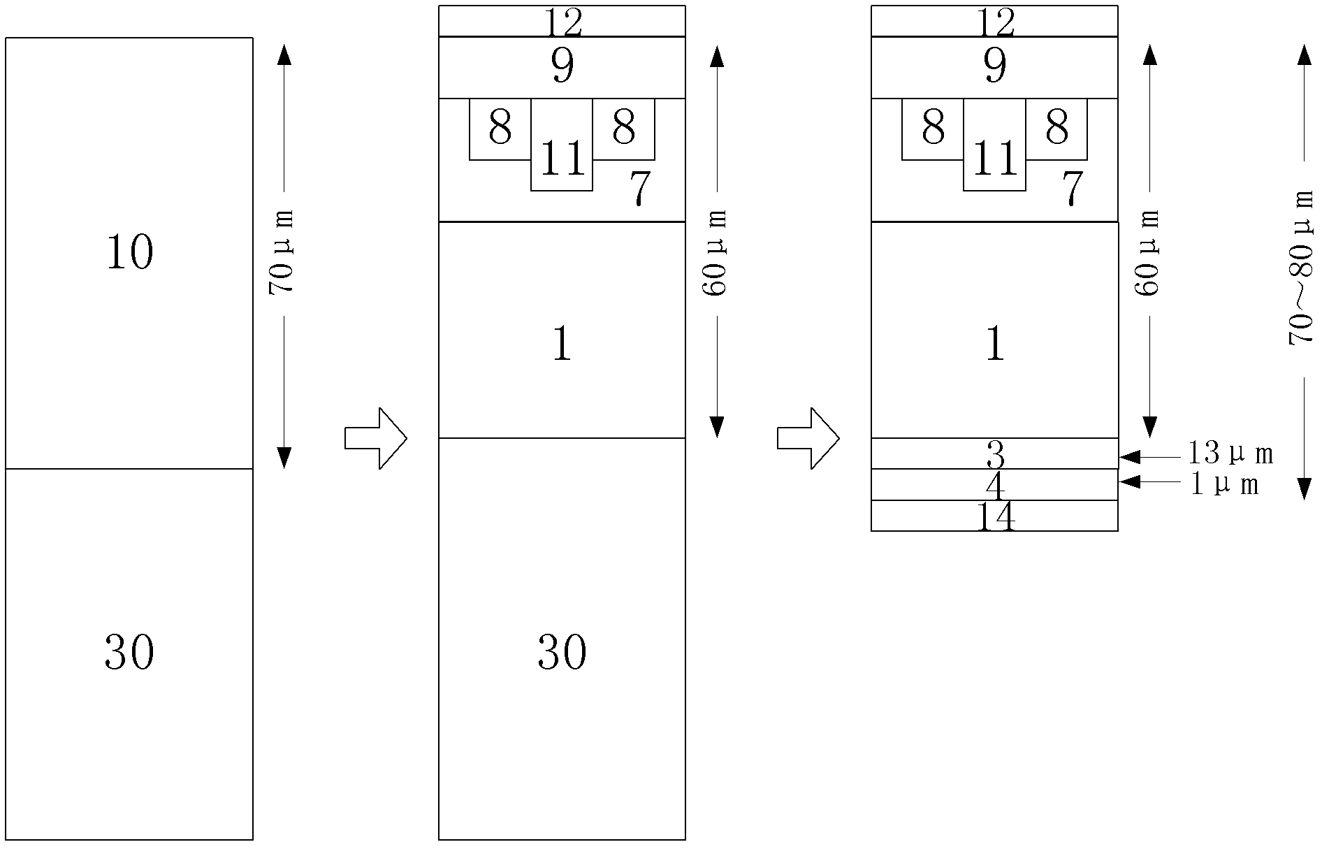
[0022] see image 3 , the method of the present invention to manufacture field-stop type IGBT device with the substrate that has epitaxial layer is:

[0023] In step 1, a silicon substrate 30 having an epitaxial layer 10 is selected.

[0024] The epitaxial layer 10 is preferably n-type medium and low doping, and the doped n-type impurity is phosphorus, for example, and the doping concentration is 1×10 11 ~1×10 14 atoms per cubic centimeter, preferably 6.5×10 13 Atoms per cubic centimeter, the epitaxial layer 10 has a thickness of 40-300 μm, preferably 70 μm. The epitaxial layer 10 can also be undoped or p-type doped.

[0025] The silicon substrate 30 is preferably n-type heavily doped silicon, and the doped n-type impurity is phosphorus, for example, with a doping concentration of 1×10 14 ~1×10 17 atoms per cubic centimeter, preferably 3×10 16 atoms per cubic centimeter. The silicon substrate 30 can also be undoped or p-type doped.

[0026] Fabricate the front structu...


PUM


Abstract

The invention discloses a method of manufacturing a field termination type insulated gate bipolar translator (IGBT) component with a substrate provided with an outward-extending layer. The method comprises the steps of selecting the substrate provided with the outward-extending layer, and manufacturing a front face structure of the IGBT component on the front face of outward-extending layer until depositing front face metal as an emission electrode; thinning the silicon base from the back face, forming a p-shaped heavy doping field blocking-up zone on the back face of the silicon base through technology of injecting ions, and depositing metal on the back face of the p-shaped heavy doping field blocking-up zone to form a collector. The method of manufacturing the IGBT component with the substrate provided with the outward-extending layer does not need production technology for extremely thin slices with thickness less than 70 nanometers, thereby effectively reducing the slice breaking rate of slice technology, and saving enormous cost of purchasing new machines and equipment.

Description

technical field [0001] The invention relates to a method for manufacturing an IGBT (Insulated Gate Bipolar Transistor, insulated gate bipolar transistor) device. Background technique [0002] The IGBT device is composed of a MOS transistor and a PNP bipolar transistor, and can also be regarded as composed of a VDMOS (Vertical double diffused MOSFET, vertical double diffused MOS transistor) and a diode. [0003] see figure 1 , which is a structural schematic diagram of a field stop (Field stop) IGBT device. On the back of the silicon wafer is a metal layer 14 as a collector, above which there is a p-type heavily doped collector region 4, further upward is an n-type heavily doped field blocking region 3, and further upward is an n-type medium and low doped region 1. There is a p well 7 in the n-type medium and low doping region 1 . The p well 7 has an n-type heavily doped source region 8 and a p-type heavily doped contact region 11 . There is a gate oxide layer 5 , an int...

Claims


Application Information

Patent Timeline
Patent Type & Authority Applications(China)
IPC IPC(8): H01L21/331H01L21/265
Inventor 张朝阳李江华房宝青颜树范
Owner SHANGHAI HUAHONG GRACE SEMICON MFG CORP
Why Eureka
Try Eureka