Array substrate and manufacturing method thereof and X ray flat plate detector

An array substrate and substrate technology, applied in the field of X-ray flat panel detectors, array substrates and manufacturing methods thereof, can solve the problems of reducing the number and density of carriers, weak stability of thin film transistors, and low carrier migration rate, etc. Achieve the effects of increasing the number and concentration, facilitating conduction, and reducing the capture effect

An array substrate and substrate technology, applied in the field of X-ray flat panel detectors, array substrates and manufacturing methods thereof, can solve the problems of reducing the number and density of carriers, weak stability of thin film transistors, and low carrier migration rate, etc. Achieve the effects of increasing the number and concentration, facilitating conduction, and reducing the capture effect

CN103137641AActive Publication Date: 2013-06-05BEIJING BOE OPTOELECTRONCIS TECH CO LTD

Image

  • Array substrate and manufacturing method thereof and X ray flat plate detector
  • Array substrate and manufacturing method thereof and X ray flat plate detector
  • Array substrate and manufacturing method thereof and X ray flat plate detector

Examples


Embodiment Construction

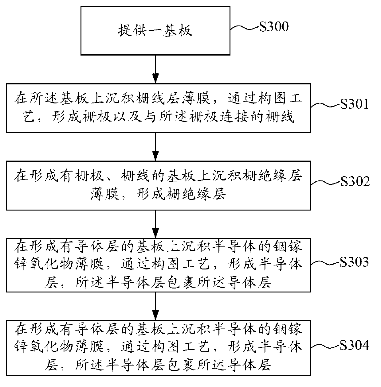
[0032] The following will clearly and completely describe the technical solutions in the embodiments of the present invention with reference to the accompanying drawings in the embodiments of the present invention. Obviously, the described embodiments are only some, not all, embodiments of the present invention. Based on the embodiments of the present invention, all other embodiments obtained by persons of ordinary skill in the art without creative efforts fall within the protection scope of the present invention.

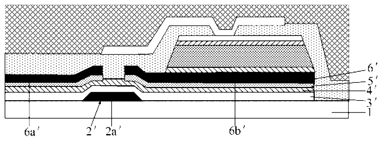
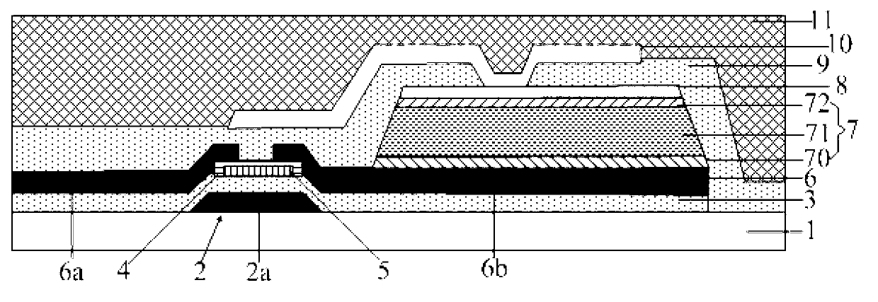
[0033] Such as figure 2 As mentioned above, it is a specific embodiment of the array substrate of the present invention, and the array substrate includes:

[0034] Substrate 1;

[0035] A gate line layer 2 formed on the substrate 1, the gate line layer 2 comprising a gate 2a and a gate line (not shown) connected to the gate 2a;

[0036] a gate insulating layer 3 formed above the gate line layer 2;

[0037] an active layer formed over the insulating layer;

[0...


PUM


Abstract

The invention discloses an array substrate and a manufacturing method of the array base plate and an X ray flat plate detector. The invention relates to the technical field of photoelectricity. Stability of a thin film transistor is strengthened. The array substrate comprises a base plate, a grid line layer, a grid insulating layer, a source layer and a data line layer. The grid line layer is formed on the substrate. The grid line layer comprises a grid electrode and a grid line connected with the grid electrode. The grid insulating layer is formed above the grid line layer. The source layer is formed above the insulating layer. The data line layer is formed above the source layer. The data line layer comprises a source electrode, a drain electrode and a data line connected with the source electrode. The data line crosses with the grid line. The source layer comprises a conductor layer and a semiconductor layer. The conductor layer is formed above the grid insulating layer. The conductor layer is packed by the semiconductor layer. The array substrate and a manufacturing method of the array substrate are mainly suitable for the X ray flat plate detector.

Description

technical field [0001] The invention relates to the field of optoelectronic technology, in particular to an array substrate, a manufacturing method thereof, and an X-ray flat panel detector. Background technique [0002] At present, the common amorphous silicon X-ray flat panel detector is an X-ray detector with an amorphous silicon photodiode array as the core. The X-ray detector includes an array substrate, which includes a thin film transistor (TFT, Thin Flim Transistor) and a photodiode. Under the irradiation of X-rays, the scintillator layer or phosphor layer of the detector converts X-ray photons into visible light , and then under the action of the photodiode, the visible light is converted into an electrical signal, and the thin film transistor reads the electrical signal and outputs the electrical signal to obtain a display image. Storage and reading, so the performance of thin film transistors is particularly important at this time. [0003] Usually, the channel ...

Claims


Application Information

Patent Timeline
05 Jun 2013
Publication
CN103137641A
IPC
H01L27/146
Inventors
阎长江; 李田生