Fin type field effect transistor and forming method thereof

A technology of fin field effect transistor and fin field effect, which is applied in the direction of semiconductor devices, semiconductor/solid state device manufacturing, electrical components, etc., can solve the problems of inapplicability, achieve the purpose of increasing the driving current, increasing the carrier migration rate, The effect of simple process

Active Publication Date: 2014-03-26
SEMICON MFG INT (SHANGHAI) CORP
View PDF5 Cites 17 Cited by
  • Summary
  • Abstract
  • Description
  • Claims
  • Application Information

AI Technical Summary

Problems solved by technology

However, with the development of semiconductor technology, such as the nitride cap layer (Nitride-Cap) stress layer, due to the high dielectric constant will increase the parasitic capacitance in the device, it is no longer suitable for highly integrated fin field effect transistor technology

Method used


Image

  • Fin type field effect transistor and forming method thereof
  • Fin type field effect transistor and forming method thereof
  • Fin type field effect transistor and forming method thereof

Examples


Embodiment Construction

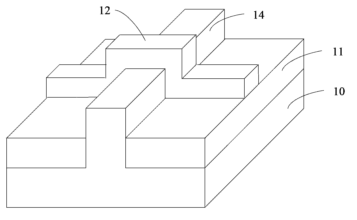
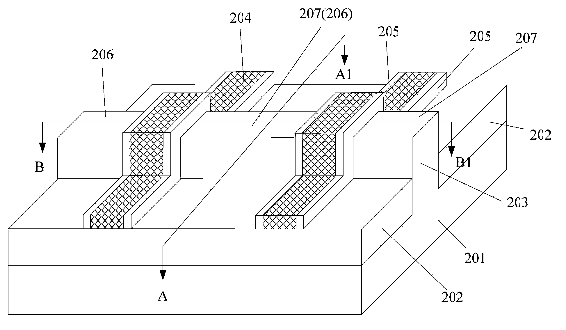
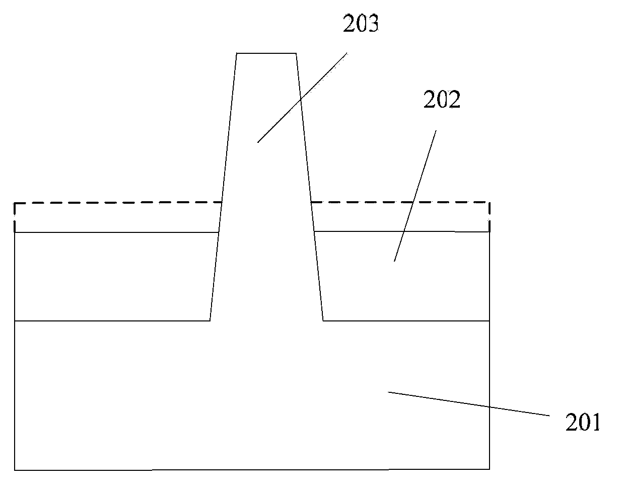
[0029] It can be known from the background art that in order to improve the performance of the fin field effect transistor device, stress can be introduced into the channel region of the MOS transistor to increase the mobility of carriers. However, with the development of semiconductor technology, such as the nitride capping layer (Nitride-Cap) stress layer, due to the high dielectric constant will increase the parasitic capacitance in the device, and the high parasitic capacitance will cause signal delay in the device and affect the chip performance. , so the use of the nitride cap layer stress layer is no longer suitable for highly integrated fin field effect transistor processes. The device performance of the fin field effect transistor in the prior art needs to be further improved.

[0030] In order to solve the above problems, the inventors of the present invention propose a method for forming a FinFET. The advantages of the present invention will become clearer by descr...


PUM


Abstract

The invention relates to a fin type field effect transistor and a forming method thereof. The fin type field effect transistor comprises a semiconductor substrate, a fin part, first dielectric layers, a gate structure, a source region, a drain region and contact metal layers, wherein the fin part is positioned on the surface of the semiconductor substrate; the first dielectric layers are positioned on two sides of the fin part, and the surfaces of the first dielectric layers are lower than the top of the fin part; the gate structure is positioned on the fin part and covers parts of the top and the side wall of the fin part; the source region and the drain region are positioned on two sides of the gate structure; the contact metal layers are positioned on the surfaces of the source region and the drain region and have stretching stress. The carrier mobility of the fin type field effect transistor is high.

Description

technical field [0001] The invention relates to the technical field of semiconductors, in particular to a fin field effect transistor and a forming method thereof. Background technique [0002] MOS transistors generate switching signals by regulating the current through the channel region by applying a voltage to the gate. However, when the semiconductor technology enters the node below 30 nanometers, the control ability of the traditional planar MOS transistor to the channel current becomes weak, causing serious leakage current. A Fin Field Effect Transistor (Fin FET) is an emerging multi-gate device, which generally includes a semiconductor fin with a high aspect ratio, a gate structure covering part of the top and sidewalls of the fin, and in the Channel regions and source / drain regions of transistors are formed in the fins. [0003] figure 1 A schematic diagram of a three-dimensional structure of a fin field effect transistor in the prior art is shown. Such as figur...

Claims


Application Information

Patent Timeline
Patent Type & Authority Applications(China)
IPC IPC(8): H01L21/336H01L21/28H01L29/78H01L29/417
CPCH01L29/16H01L29/45H01L29/452H01L29/456H01L29/66795H01L29/7842H01L29/7845H01L29/785
Inventor 三重野文健
Owner SEMICON MFG INT (SHANGHAI) CORP
Why Eureka
Try Eureka