Strobing device unit used for cross array integration way of double-pole type resistance change storage

A technology of resistive memory and gating devices, which is applied in the field of microelectronics, can solve the problems that rectifier diodes cannot meet the current requirements and cannot provide sufficient current, and achieve the effects of suppressing read crosstalk, high current density, and reducing read crosstalk

Inactive Publication Date: 2013-06-05
INST OF MICROELECTRONICS CHINESE ACAD OF SCI
View PDF5 Cites 12 Cited by
  • Summary
  • Abstract
  • Description
  • Claims
  • Application Information

AI Technical Summary

Problems solved by technology

However, usually the rectifier diode only has forward conduction characteristics and cannot provide enough current in the reverse direction. Therefore, the current resistive memory that can be integrated with the rectifier diode must have unipolar resistance transition characteristics, that is, the programming and switching characterist...

Method used


Image

  • Strobing device unit used for cross array integration way of double-pole type resistance change storage
  • Strobing device unit used for cross array integration way of double-pole type resistance change storage
  • Strobing device unit used for cross array integration way of double-pole type resistance change storage

Examples


Embodiment Construction

[0034] In order to make the object, technical solution and advantages of the present invention clearer, the present invention will be described in further detail below in conjunction with specific embodiments and with reference to the accompanying drawings.

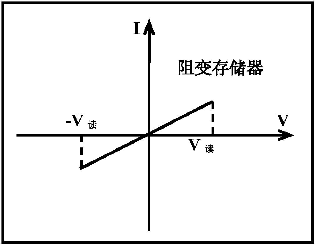
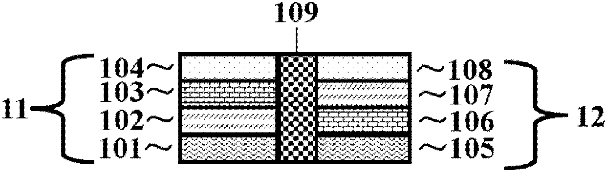
[0035] Such as image 3 as shown, image 3 A schematic diagram of the unit structure of a gating device suitable for bipolar resistive memory cross-array integration provided by the present invention, the gating device unit includes an n-p diode 11 and a p-n diode 12, the n-p diode 11 and the p-n diode 12 The polarities of the gates are reversed and connected in parallel, so that the gating device unit has bidirectional rectification characteristics.

[0036] Wherein, the n-p diode 11 and the p-n diode 12 are connected in parallel through a dielectric isolation layer 109 . The material used for the dielectric isolation layer 109 is SiO 2 、Si 2 N 3 ,, HfO 2 , ZrO 2 or Al 2 o 3 One of.

[0037] The n-p diode 11 in...


PUM

PropertyMeasurementUnit
Thicknessaaaaaaaaaa
Thicknessaaaaaaaaaa

Abstract

The invention discloses a strobing device unit used for a cross array integration way of a double-pole type resistance change storage. The strobing device unit used for the cross array integration way of the double-pole type resistance change storage is characterized in that the strobing device unit comprises an n-p diode and a p-n diode. Polarity of the n-p diode and polarity of the p-n diode are opposite. The polarity of the n-p diode is in parallel connection with polarity of the p-n diode. The strobing device unit is has the feature of the two-way rectification. The strobing device unit used for the cross array integration way of the double-pole type resistance change storage has the feature of the two-way rectification. High electric current density can be provided of the random voltage polarity in the brakeover-state. Rectification ratio (RV2/RV) is provided in the read-voltage. The phenomenon of read-interference in the double-pole type resistance change storage cross array structure can be restrained. Misreading is avoided. The problem that the common rectification diode is only suitable for the single-pole type resistance change storage cross array is solved.

Description

technical field [0001] The invention relates to the technical field of microelectronics, in particular to a gating device unit applicable to a cross-array integration mode of a bipolar resistive memory. Background technique [0002] Resistance random access memory (resistive random access memory, RRAM) is an emerging non-volatile storage technology, in terms of device structure, cell area, storage density, power consumption, programming / erasing speed, 3D integration and multi- It has great advantages in many aspects such as value storage, and has become one of the most powerful competitors to replace the mainstream product "flash memory" in the current non-volatile storage technology market. The sandwich structure of metal / insulator / metal (MIM) is the basic structure of RRAM, and this vertical MIM structure is beneficial to realize ultra-high-density storage by means of cross-array integration. In the interleaved array structure, the vertical parallel intersections contain ...

Claims


Application Information

Patent Timeline
IPC IPC(8): H01L27/24H01L45/00G11C13/00
CPCG11C13/0069G11C2013/0054G11C13/004G11C13/003G11C13/0007H01L27/24H01L29/861G11C2213/15G11C13/0023G11C2013/0073H01L45/00H10B63/20H10N70/20H10N70/8833H10B63/80H10N70/24H10N70/841H10N70/884H10N70/8265
Inventor 刘琦刘明龙世兵吕杭炳王艳
Owner INST OF MICROELECTRONICS CHINESE ACAD OF SCI
Why Eureka
Try Eureka