Thin film transistor array substrate, display device and method

A thin-film transistor and array substrate technology, which is applied in the field of thin-film transistor liquid crystal display manufacturing, can solve problems such as large longitudinal noise electric field, weak liquid crystal alignment ability, liquid crystal deflection disorder, etc., and achieve reduction in size, weakening longitudinal noise electric field, and enhanced alignment ability Effect

Inactive Publication Date: 2013-06-12
BOE TECH GRP CO LTD +1
View PDF5 Cites 10 Cited by
  • Summary
  • Abstract
  • Description
  • Claims
  • Application Information

AI Technical Summary

Problems solved by technology

[0003] For existing display substrate manufacturing technologies, 1 st Transparent conductive film as pixel electrode, comb 2 nd Transparent conductive film as common electrode, comb 2 nd A gap is formed between each slit of the transparent conductive film. Under the joint action of the left and right strip electrodes, the above-mentioned horizontal electric field becomes very small in the middle area of ​​the gap, the vertical noise electric field becomes larger, and the orientation ability of the horizontal electric field to the liquid crystal becomes very large. Weak, pressing in the white state screen causes liquid crystal deflection to be chaotic, and the weak horizontal electric field in the middle area of ​​the gap cannot restore the deflection state of the liquid crystal before pressing, which causes Trace Mura (defects such as residual pressing traces) to occur; With increasing density, 2 nd The strip width of the transparent conductive film becomes smaller and smaller, and this problem becomes more and more serious when the gap width does not change significantly

Method used


Image

  • Thin film transistor array substrate, display device and method
  • Thin film transistor array substrate, display device and method
  • Thin film transistor array substrate, display device and method

Examples


Embodiment Construction

[0038] The specific implementation manners of the present invention will be further described in detail below in conjunction with the accompanying drawings and embodiments. The following examples are used to illustrate the present invention, but are not intended to limit the scope of the present invention.

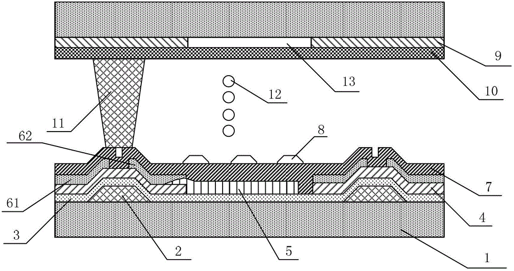
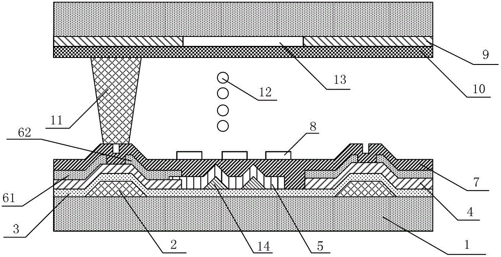
[0039] In order to solve the occurrence of Trace Mura in the existing display substrate manufacturing technology, the present invention proposes a thin film transistor array substrate,

[0040] A thin film transistor array substrate, including a base substrate, and a thin film transistor formed on the base substrate, a second insulating layer, a first electrode, and a second electrode;

[0041] Wherein, the first electrode and the second electrode are used to form an electric field, and the second insulating layer is located between the first electrode and the second electrode;

[0042] The second electrode is a comb electrode and is located on a side of the second insula...


PUM

PropertyMeasurementUnit
angleaaaaaaaaaa
thicknessaaaaaaaaaa

Abstract

The invention discloses a thin film transistor array substrate, a display device and a method in the field of thin film transistor liquid crystal display manufacture. The thin film transistor array substrate comprises a backing substrate, bump structures, and thin film transistors, a second insulation layer, first electrodes and second electrodes that are formed on the backing substrate, wherein the first electrodes and the second electrodes are used for forming an electric field; the second insulation layer is positioned among the first electrodes and the second electrodes; the second electrodes are comb-shaped electrodes, and positioned on one side of the second insulation layer far from the backing substrate; the bump structures are positioned on one side of each first electrode close to the backing substrate; and positions of the bump structures correspond to gaps among the comb-shaped electrodes. According to the thin film transistor array substrate, the display device and the method, a shape of a pixel electrode layer is changed by a resin block, so that sizes of horizontal electric field weakening areas among the public electrodes are reduced effectively; a longitudinal noise electric field is weakened; the orientation capability of the horizontal electric field to liquid crystals is improved; Trace Mura is avoided; and the quality of a display is improved.

Description

technical field [0001] The invention relates to the field of manufacturing thin film transistor liquid crystal displays, in particular to a thin film transistor array substrate, a display device and a method. Background technique [0002] TFT-LCD, Thin Film Transistor (TFT for short) Liquid Crystal Display (LCD for short) basic structure includes array substrate (Array Substrate) and color filter substrate (CF Substrate), and filled between the two substrates The liquid crystal layer (LC) between the array substrate and the color filter substrate has a polyimide film layer (alignment film layer) (Polyimide film, referred to as: PIfilm) that has an alignment effect on the liquid crystal. The array substrate includes a gate, a gate insulating layer, an active layer, a source and a drain. In the existing display substrate manufacturing technology, a gate electrode, a gate insulating layer, an active layer, a pixel electrode, a source-drain electrode, a second insulating layer,...

Claims


Application Information

Patent Timeline
Patent Type & Authority Applications(China)
IPC IPC(8): G02F1/1362G02F1/1368G02F1/1343H01L27/12H01L21/77
CPCG02F1/1362H01L27/124G02F1/133707G02F1/13394H01L27/1248G02F1/134363H01L27/1259G02F1/134318G02F1/133345G02F1/134336G02F1/1368H01L29/41733H01L29/42384
Inventor 胡伟莫再隆石天雷
Owner BOE TECH GRP CO LTD
Why Eureka
Try Eureka