Manufacturing method for flip chip gold bumps

A technology of flip-chip and bumps, which is applied in semiconductor/solid-state device manufacturing, electrical components, electrical solid-state devices, etc. The need for mass production, the difficulty of obtaining nail-head bumps and other issues, to achieve the effect of improving production efficiency, avoiding damage, and improving reliability

Inactive Publication Date: 2013-06-12
PEKING UNIV SHENZHEN GRADUATE SCHOOL
View PDF10 Cites 8 Cited by
  • Summary
  • Abstract
  • Description
  • Claims
  • Application Information

AI Technical Summary

Problems solved by technology

In addition, for relatively brittle materials such as GaAs materials, the adhesion of the pads is small, and it is difficult to obtain good stud bumps
Moreover, the method of making nail-head Au bumps cannot meet the needs of mass production of multiple terminals, and it is difficult to ensure the uniformity of the shape of the bumps and the consistency of electrical contact performance.

Method used


Image

  • Manufacturing method for flip chip gold bumps
  • Manufacturing method for flip chip gold bumps
  • Manufacturing method for flip chip gold bumps

Examples


Embodiment Construction

[0027] A method for preparing flip-chip gold bumps, as shown in the figure, comprises the following steps:

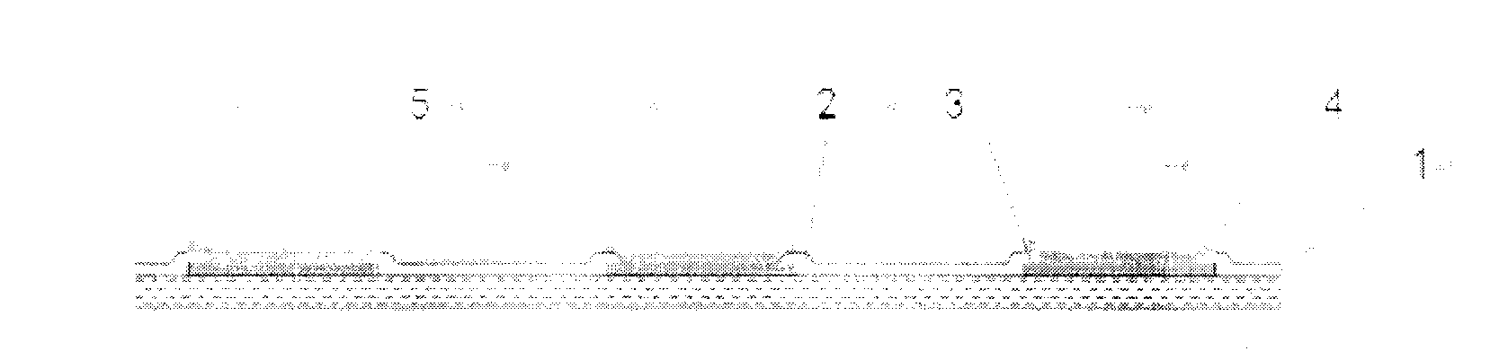
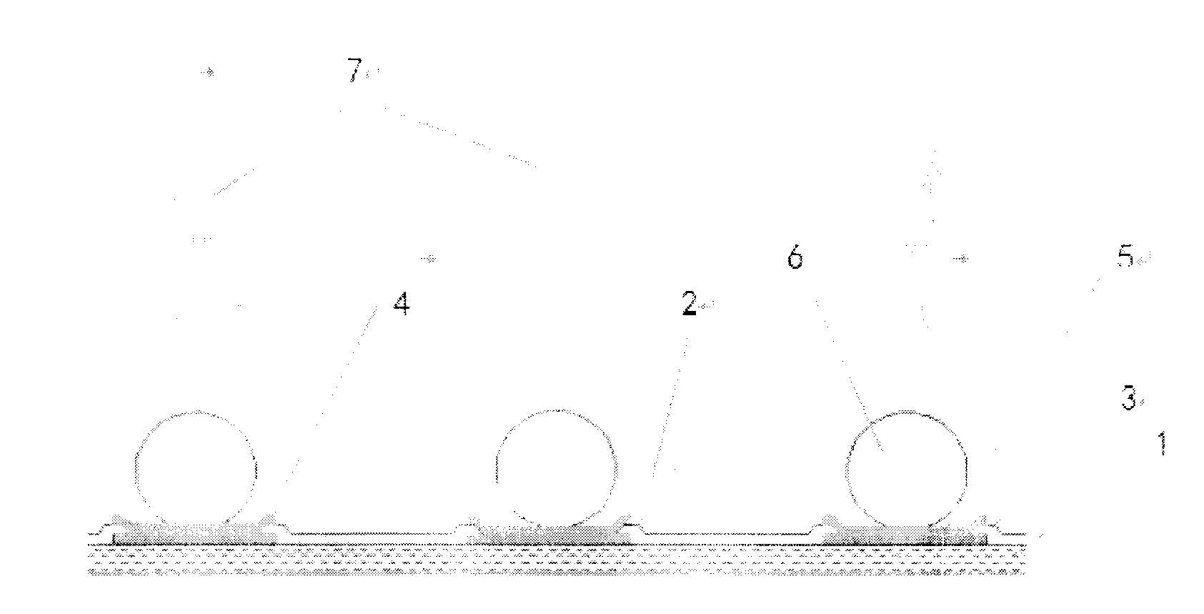
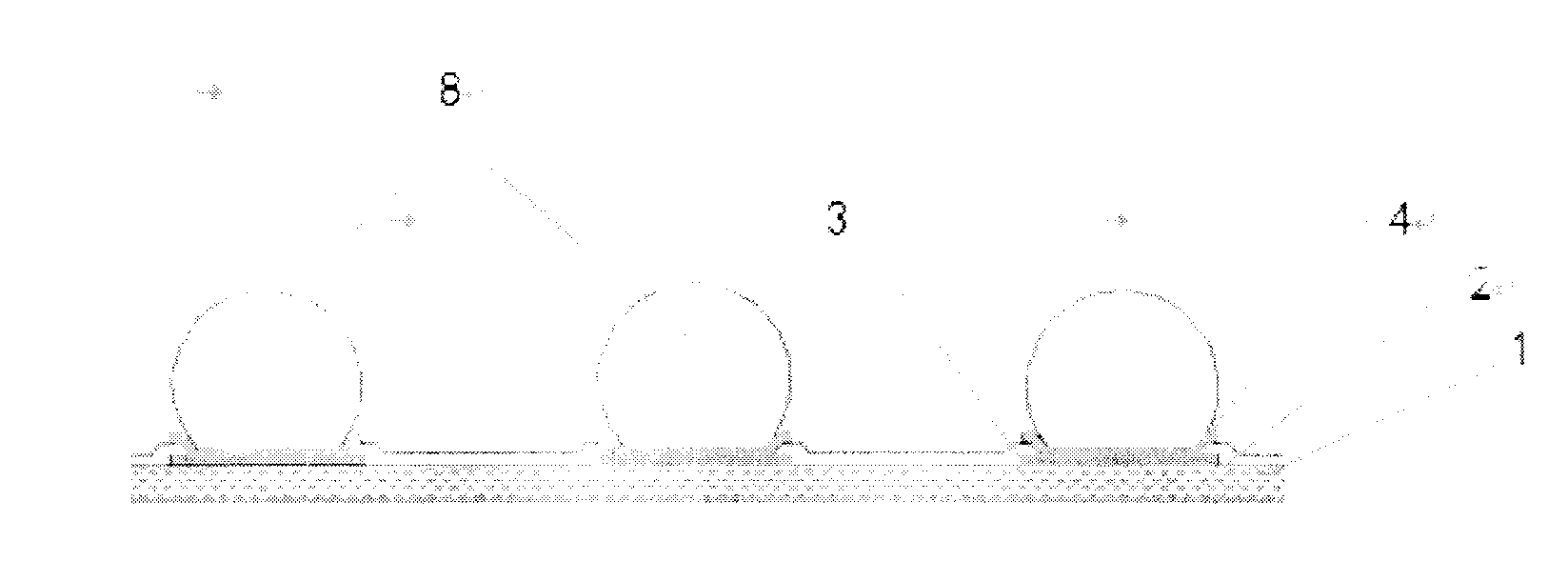
[0028] Such as figure 1 As shown, the invention evenly smears flux on the UBM coating 4 of the chip 1 pad. This technical solution uses high-viscosity flux to play the role of bonding and flux, and to ensure that the pattern of flux after printing is clear and does not flow . A special small template is used for printing. Usually, the thickness of the template and the size of the opening are determined according to the ball diameter and pitch. The thickness of the template is about one tenth of the ball diameter, and the opening size is slightly larger than the radius of the ball. According to the size requirements of the gold bumps, select gold nanospheres with a suitable diameter, and the size of the gold balls is on the order of tens of nanometers to microns. Using a ball planter, select a matching template. The opening size of the template should be 0.05-0.1mm lar...


PUM


Abstract

The invention belongs to the field of semiconductor package and discloses a manufacturing method for flip chip gold bumps. The method includes the following steps: by utilization of screen printing method, scaling powder with high viscosity is printed on an electrode under bump metal (UBM) plating layer; by utilization of a ball placing device, a matched template is chosen, gold balls are placed on a weld plating layer and the situation that the gold balls are adhered to the chip electrode UBM plating layer is ensured; and by utilization of lasers, the gold balls are re-melted, appropriate irradiation time and power are chosen, and the gold bumps are obtained and meet the shape requirement and requirements of electricity and mechanical performance. By utilization of laser braze, the manufacturing method for the flip chip gold bumps has the unique advantages of being capable of heating locally and quickly, cooling quickly and the like. The laser input power and the laser irradiation time are controlled, the gold bumps with optimal bump shapes, the mechanical performance and the electricity performance are obtained.

Description

technical field [0001] The invention relates to the field of semiconductor packaging, in particular to a method for manufacturing flip-chip gold bumps. Background technique [0002] In recent years, the two industries of flat panel displays and portable electronic products have developed rapidly. Electronic products such as mobile phones, electronic dictionaries, and digital cameras have become indispensable products in the daily life of modern people due to their small size, multi-functions, and ease of use. Large flat-panel displays have the advantages of lightness, thinness, no radiation and high resolution, and are gradually replacing traditional TVs and monitors. Whether it is a small mobile phone display or a large LCD monitor, driver chips are required. The LCD driver is characterized by a small chip area but a large number of I / O terminals. Obviously, the traditional IC packaging technology cannot meet the requirements of portable electronic products for short, thi...

Claims


Application Information

Patent Timeline
Patent Type & Authority Applications(China)
IPC IPC(8): H01L21/60
CPCH01L24/11H01L2224/11H01L2924/00015H01L2924/15787H01L2924/00H01L2224/1134H01L2924/00012
Inventor 刘葳金鹏
Owner PEKING UNIV SHENZHEN GRADUATE SCHOOL
Why Eureka
Try Eureka