The Trigger Circuit Structure of IC Power Rail Antistatic Protection

An integrated circuit and electrostatic protection technology, applied in the electronic field, can solve the problems of large leakage current and high chip power consumption, achieve the effects of small leakage current, reduce trigger voltage, and improve ESD capability

Inactive Publication Date: 2015-07-29
UNIV OF ELECTRONICS SCI & TECH OF CHINA
View PDF4 Cites 2 Cited by
  • Summary
  • Abstract
  • Description
  • Claims
  • Application Information

AI Technical Summary

Problems solved by technology

However, under the advanced CMOS process, the area of ​​the capacitor is much larger than the area of ​​the transistor, and due to the influence of its parasitic resistance, the capacitor cannot completely block the current, and the ESD protection device will be weakly turned on, which will cause a large Leakage current, resulting in higher power consumption when the chip is working

Method used


Image

  • The Trigger Circuit Structure of IC Power Rail Antistatic Protection
  • The Trigger Circuit Structure of IC Power Rail Antistatic Protection
  • The Trigger Circuit Structure of IC Power Rail Antistatic Protection

Examples


specific Embodiment approach 1

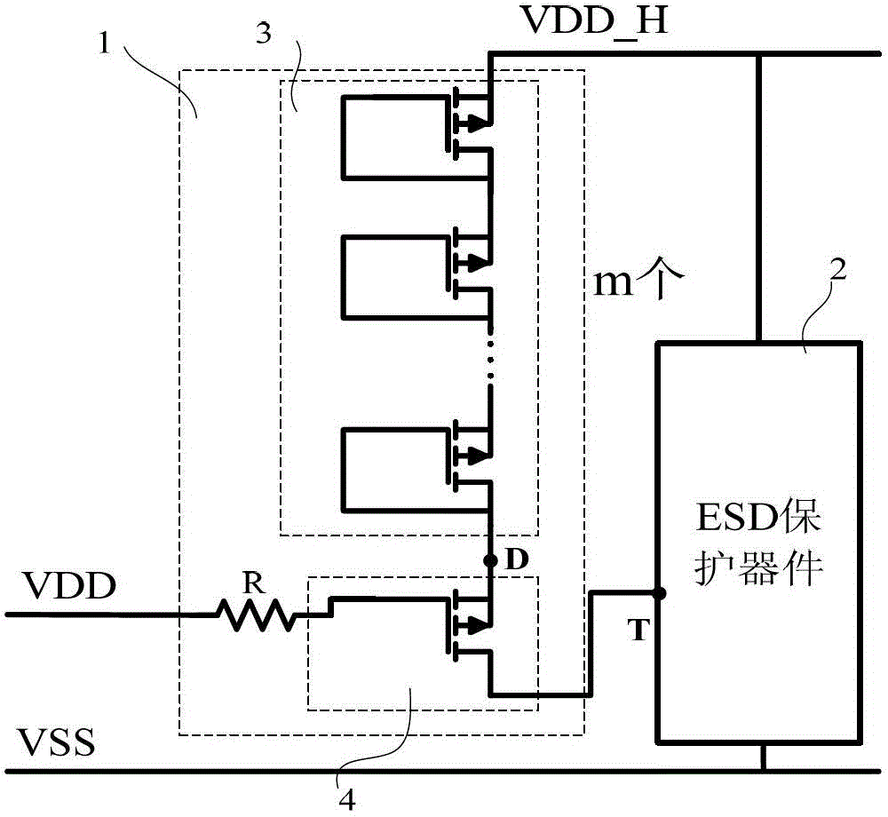
[0016] Trigger circuit structure 1 for integrated circuit power rail anti-static protection, used to trigger integrated circuit high-voltage power rail anti-static protection devices with mixed operating voltages, such as image 3 As shown, it includes a diode-connected series circuit 3 composed of m (m is a positive integer) first PMOS transistors, a second PMOS transistor 4 and a resistor R; the diode connection formed by the m first PMOS transistors In the series circuit 3 of the form, the gate of each first PMOS transistor is connected to the drain, the substrate is connected to the source, and the source of each first PMOS transistor is connected to the drain of a first PMOS transistor above it; The source of the two PMOS transistors 4 is short-circuited to the substrate, and then connected to the drain of the bottom first PMOS transistor in the series circuit 3 of the diode connection form formed by m first PMOS transistors; the gate of the second PMOS transistor 4 It is...

specific Embodiment approach 2

[0022] The structure of the second embodiment is that an NMOS transistor 5 is added on the basis of the first embodiment, such as Figure 5 As shown, an NMOS transistor 5 is connected under the PMOS transistor 4 . The source of the NMOS transistor 5 is short-circuited to the substrate and connected to the ground rail VSS, the drain of the NMOS transistor 5 is connected to the drain of the second PMOS transistor 4; the gates of the NMOS transistor 5 and the PMOS transistor 4 are connected to each other through a resistor R Low Voltage Supply Rail VDD.

[0023] The function of the NMOS transistor 5 in the above scheme is: when the protected integrated circuit works normally, since the gates of the second PMOS transistor 4 and the NMOS transistor 5 are connected to the low-voltage power supply rail VDD, the second PMOS transistor 4 is turned off at this time. The NMOS transistor 5 is turned on, and the voltage of the trigger terminal of the ESD protection device 2 is pulled to a...


PUM


Abstract

The invention provides a trigger circuit structure with circuit power supply rail antistatic protection, belonging to the technical field of electronics. The structure is used for triggering an integrated circuit high voltage power supply rail antistatic protective device with mixed working voltage, and comprises a series circuit, a second PMOS (positive channel metal oxide semiconductor) tube and a resistor R, wherein the series circuit consists of m (a positive integer) first PMOS tubes and is formed by connection of diodes; the source electrode of the most top first PMOS tube in the series circuit is connected with VDD_H (voltage drain drain_high); the drain electrode of the second PMOS tube is connected with a triggering end T of an ESD (electro-static discharge) protective device; the grid electrode of the second PMOS tube is connected with VDD (voltage drain drain) through the resistor R. The trigger circuit structure consists of a low voltage device, however, the trigger circuit structure can tolerate VDD_H voltage of a high voltage power supply rail, reduce the trigger voltage of the device, promote uniform conduction of the device, and improve ESD capability, and meanwhile, no capacitor device exists in the circuit, thus, the leakage current of the protected integrated circuit under normal working is smaller.

Description

technical field [0001] The invention belongs to the field of electronic technology, and relates to the design of an electrostatic discharge (ESD for short) protection circuit for a semiconductor integrated circuit chip, in particular to a power rail for two (or more) different voltages, and is only controlled by Electrostatic protection design technology for integrated circuits composed of low-voltage devices. Background technique [0002] With the continuous development of CMOS technology, the number of transistors integrated on each chip has also increased dramatically. However, in a complex system, when different chips are connected to each other, since the working voltage of the chip may be different, its I / O interface circuit may need to receive or output signals of different voltage values. This requires the I / O interface circuits between chips to be able to withstand different voltages. However, for integrated circuits operating at low voltage, the gate oxide layer ...

Claims


Application Information

Patent Timeline
Patent Type & Authority Patents(China)
IPC IPC(8): H01L27/02
Inventor 张波樊航盛玉荣柯明道
Owner UNIV OF ELECTRONICS SCI & TECH OF CHINA
Why Eureka
Try Eureka