Plastic part and manufacturing method thereof
A manufacturing method and technology of plastic parts, applied in the direction of chemical instruments and methods, electrical components, synthetic resin layered products, etc., can solve the problems of high price, increase the cost of indium tin non-conductive film preparation, etc., to reduce production costs, Improved stability and repeatability effects
- Summary
- Abstract
- Description
- Claims
- Application Information
AI Technical Summary
Problems solved by technology
Method used
Image
Examples
Embodiment 1
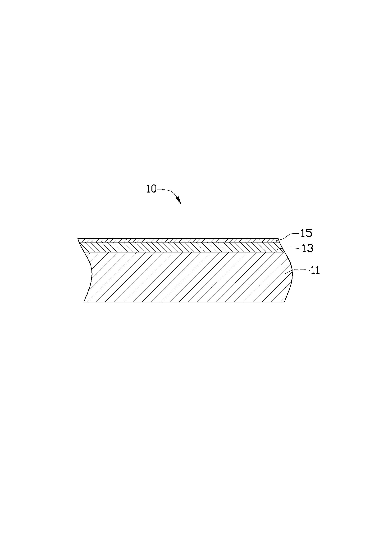
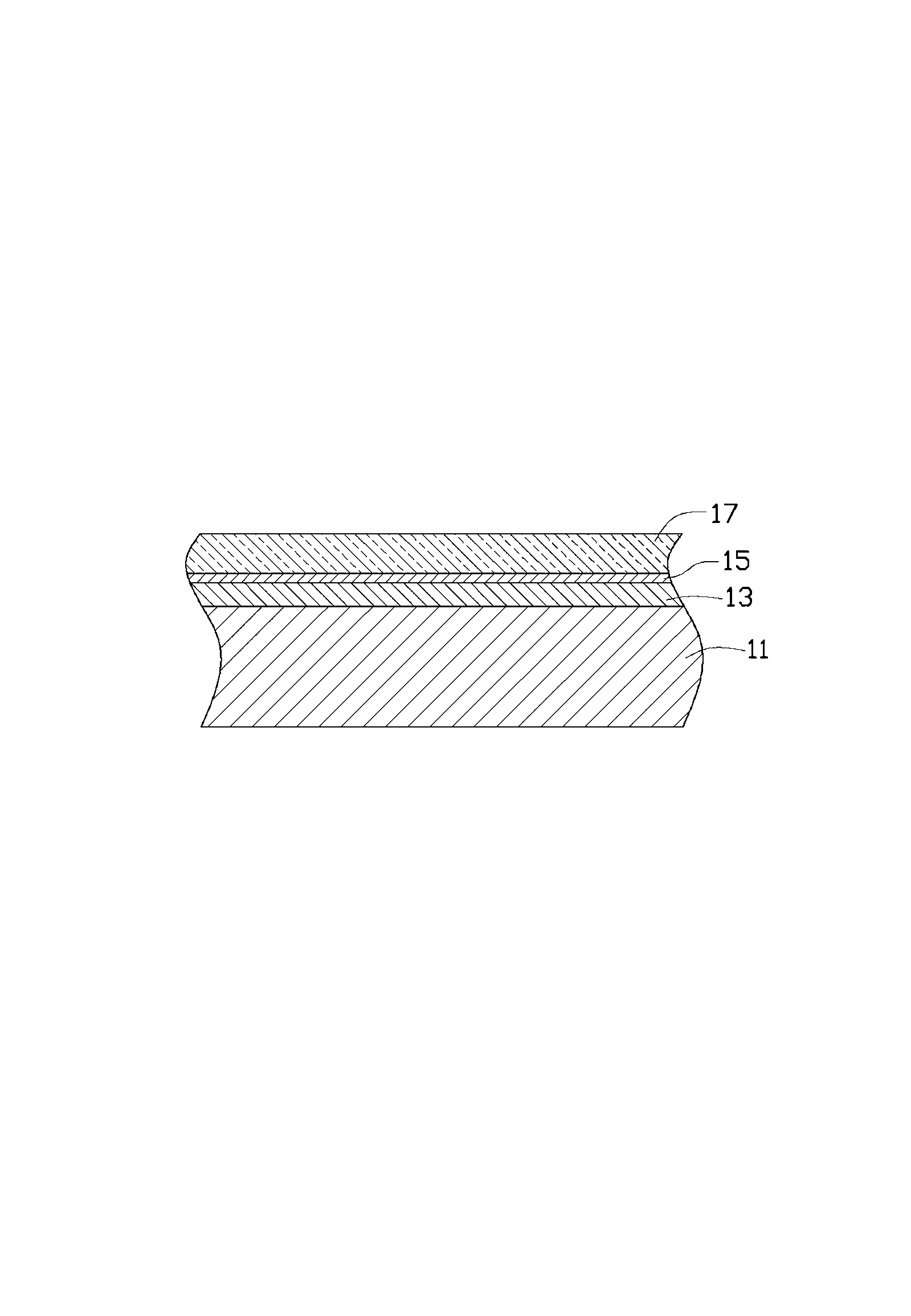
[0029] Forming the primer layer 13: The paint used to form the primer layer 13 is SPR60982 UV paint provided by PPG Industries, and the spray gun pressure is set to 1000 Pa, and the spraying distance is set to 15 cm. After the spraying is completed, the plastic substrate 11 is subjected to ultraviolet light curing treatment, the wavelength of ultraviolet light is 315nm, and the curing energy is 1300 millijoules / cm 2 , The curing time is 8min. After curing, the primer layer 13 has a thickness of 9 μm.
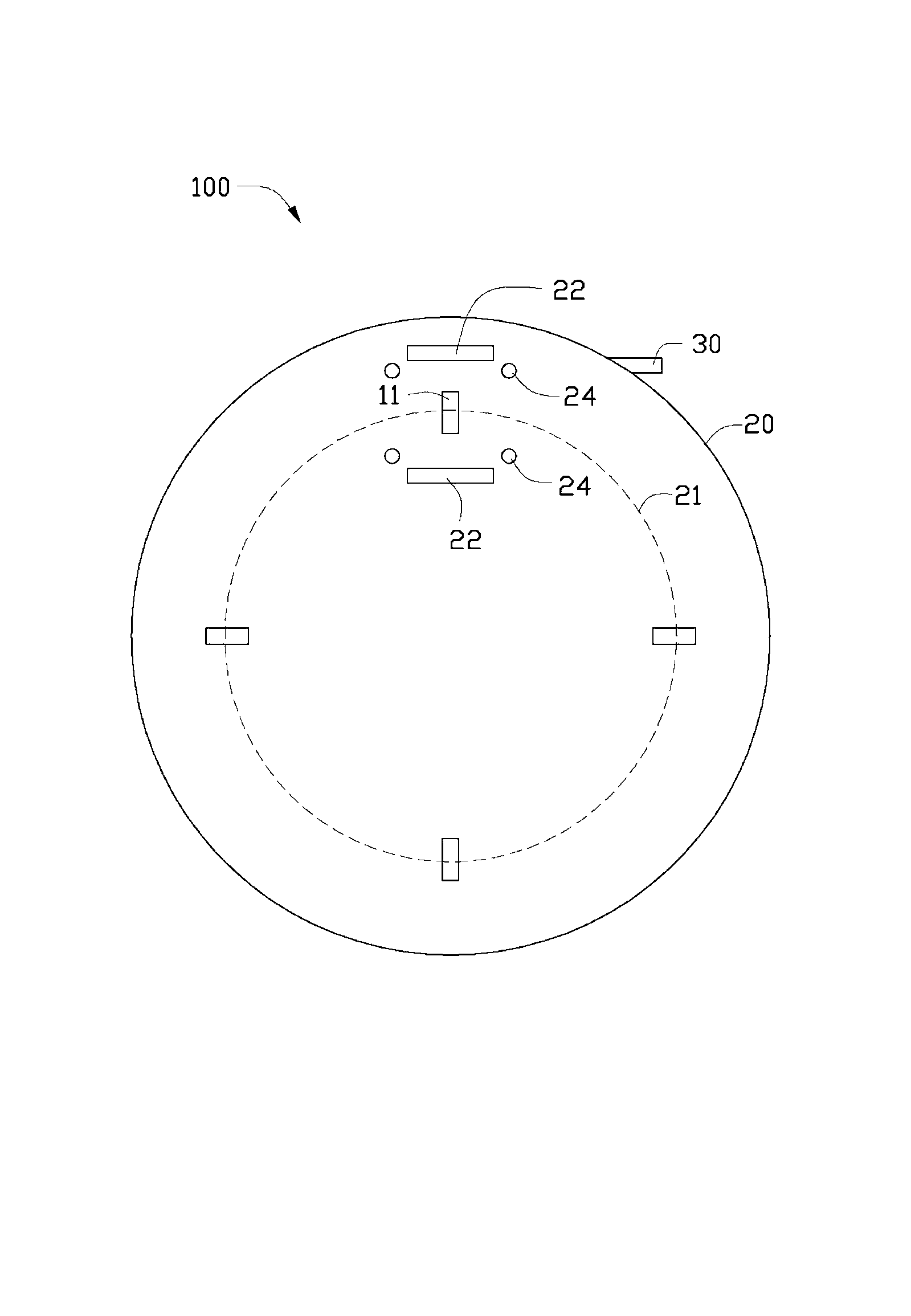
[0030] Form the non-conductive film layer 15: vacuumize the coating chamber 20 to 6.0×10 -3 Pa, set the argon gas flow rate to 180 sscm, and set the power of the silicon-aluminum composite target 22 to 8 kW; the temperature of the coating chamber 20 is room temperature, and the coating time is 3 minutes. The thickness of the non-conductive coating layer 15 is 25nm.
[0031] The chromaticity region of the non-conductive coating layer 15 has an L* coordinate of 72 in the CIE LA...
Embodiment 2
[0033] Forming the primer layer 13: The paint used to form the primer layer 13 is SPR60982 UV paint provided by PPG Industries, and the spray gun pressure is set at 1200 Pa and the spraying distance is 20 cm. After the spraying is completed, the plastic substrate 11 is subjected to ultraviolet light curing treatment, the wavelength of ultraviolet light is 315nm, and the curing energy is 1400 millijoules / cm 2 , The curing time is 10min. After curing, the primer layer 13 has a thickness of 12 μm.
[0034] Form the non-conductive film layer 15: vacuumize the coating chamber 20 to 6.0×10 -3 Pa, the argon gas flow rate is set to 200sscm, the power of the silicon-aluminum composite target 22 is 10kW; the temperature of the coating chamber 20 is room temperature, and the coating time is 2.5min. The thickness of the non-conductive coating layer 15 is 30nm.
[0035] The chromaticity region of the non-conductive coating layer 15 has an L* coordinate of 74 in the CIE LAB color system,...
PUM
| Property | Measurement | Unit |
|---|---|---|
| thickness | aaaaa | aaaaa |
| thickness | aaaaa | aaaaa |
| thickness | aaaaa | aaaaa |
Abstract
Description
Claims
Application Information


