A method of manufacturing a semiconductor packaging device

A technology for packaging devices and manufacturing methods, which is applied in the manufacture of semiconductor/solid-state devices, semiconductor devices, electric solid-state devices, etc., can solve the problem of lead frame and plastic packaging material pins or chip carriers falling off, low bonding strength between lead frame and plastic packaging material, The pins cannot complete the packaging process and other problems, so as to achieve the effects of low cost, prevention of delamination and high reliability

Active Publication Date: 2016-05-18
南通腾龙通信科技有限公司
View PDF3 Cites 0 Cited by
  • Summary
  • Abstract
  • Description
  • Claims
  • Application Information

AI Technical Summary

Problems solved by technology

[0004] With the improvement of IC integration and the continuous enhancement of functions, the number of I / Os of ICs increases, and the number of I / O pins of corresponding electronic packages also increases accordingly. The pins of the ring are arranged around the chip carrier, which limits the increase in the number of I / Os and cannot meet the needs of high-density ICs with more I / Os.
Even if the traditional QFN package with non-step structure design has multi-turn pins, it cannot effectively lock the plastic packaging material, resulting in low bonding strength between the lead frame and the plastic packaging material, which is easy to cause delamination and even lead-out of the lead frame and plastic packaging material. The feet or the chip carrier fall off, and the moisture cannot be effectively prevented from diffusing into the electronic package along the interface between the lead frame and the plastic packaging material, which seriously affects the reliability of the package.
Even if the traditional QFN package has a stepped structure design, it can only be realized based on single-turn pins or staggered multi-turn pins, and each outer end of all pins must extend to one side of the package body and be exposed to the external environment. In the middle, the moisture is easily diffused into the package, which affects the reliability of the product, and due to the limitation of space, it is impossible to achieve higher density packaging
The chip load and pins of the traditional QFN package must be based on the pre-fabricated lead frame structure, otherwise the chip load and pins cannot complete all the packaging process due to lack of mechanical support and connection
Traditional QFN packages need to paste tape on the back of the lead frame in advance to prevent overflow during the plastic sealing process.

Method used


Image

  • A method of manufacturing a semiconductor packaging device
  • A method of manufacturing a semiconductor packaging device
  • A method of manufacturing a semiconductor packaging device

Examples


Embodiment Construction

[0041] The present invention is described in detail below in conjunction with accompanying drawing:

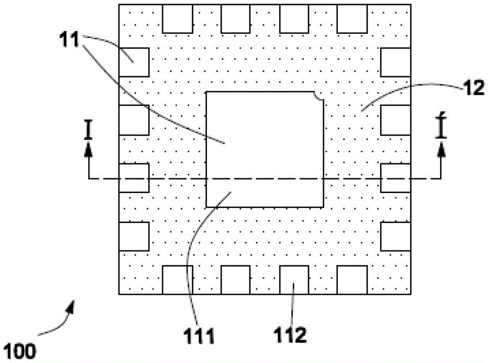
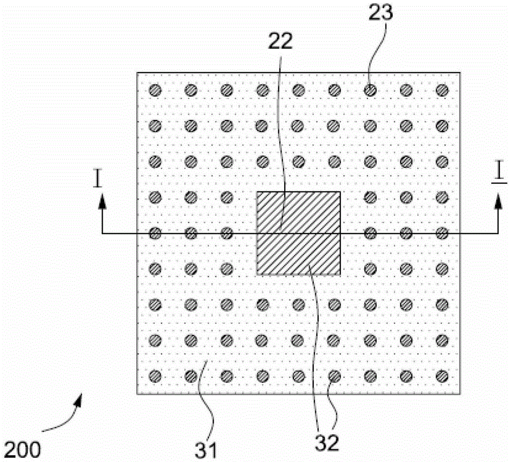
[0042] Figure 2A A schematic diagram of the back side of a QFN packaged device with a multi-circle pin arrangement in which the cross-section of the pins is circular and the pins on each side of the chip carrier are arranged in parallel according to the embodiment of the present invention.

[0043] Refer to the above Figure 2A It can be seen that in this embodiment, the QFN packaged device 200 with multi-turn pin arrangement has a chip carrier 22 and pins 23 arranged in multi-turn around the chip carrier 22, and the arrangement of the pins 23 on each side of the chip carrier 22 The method is arranged in parallel, the cross section of the pins 23 is circular, the second metal material layer 32 is disposed on the surface of the chip carrier 22 and the pins 23 , and the plastic encapsulation material 31 is disposed in the QFN package device 200 . The arrangement of the pins 2...


PUM


Abstract

The invention discloses a manufacture method of a semiconductor package component. A chip load and a pin of a quad flat non-leaded package (QFN) semiconductor package component are not manufactured based on a lead frame structure which is manufactured in advance, while the chip load and the pin which are provided with a step structure are formed by the organic integration of etching, electroplating and chemical plating methods in the process of packaging technology. Seal package is carried out by adopting of plastic package materials, and after the plastic package is finished, the independent chip load and the pin are formed by adopting an etching method or a mechanical grinding method.

Description

technical field [0001] The invention relates to the technical field of manufacturing semiconductor components, in particular to a method for manufacturing a quadrilateral flat no-lead package with high I / O density. Background technique [0002] With the development of electronic products such as mobile phones and notebook computers towards miniaturization, portability, ultra-thinness, multimedia and low-cost requirements for popularization, high-density, high-performance, high-reliability and low-cost packaging forms and Its assembly technology has been developed rapidly. Compared with expensive BGA and other packaging forms, the new packaging technology that has developed rapidly in recent years, that is, the quad flat non-lead QFN (QuadFlatNon-leadPackage) package, has good thermal and electrical properties, small size, low cost and Many advantages such as high productivity have triggered a new revolution in the field of microelectronic packaging technology. [0003] Fi...

Claims


Application Information

Patent Timeline
Patent Type & Authority Patents(China)
IPC IPC(8): H01L21/50H01L21/56H01L21/60
CPCH01L24/97H01L2224/32245H01L2224/48091H01L2224/48095H01L2224/48247H01L2224/48257H01L2224/73265H01L2224/92247H01L2224/97H01L2924/181
Inventor 秦飞夏国峰安彤刘程艳武伟朱文辉
Owner 南通腾龙通信科技有限公司
Why Eureka
Try Eureka