Test component used in complementary metal-oxide-semiconductor transistor (CMOS) component and manufacture method and using method thereof

A technology for testing devices and devices, which is applied in the direction of single semiconductor device testing, semiconductor/solid-state device testing/measurement, semiconductor/solid-state device manufacturing, etc. Production cost, the effect of improving the yield rate

Active Publication Date: 2013-06-19
SEMICON MFG INT (SHANGHAI) CORP
View PDF5 Cites 4 Cited by
  • Summary
  • Abstract
  • Description
  • Claims
  • Application Information

AI Technical Summary

Problems solved by technology

[0003] However, when forming the N-type doped region of the NMOS device, if the edge of the photoresist layer 102 covering the N-type well region crosses the boundary A between the N-type well region and the P-type well region and enters the P-type well region, Then it will lead to the formation of doping loss in the covered area of ​​the P-type well region. This doping loss will cause the static leakage current to be 3-10 times higher than the standard value, and usually occurs in the central area of ​​the wafer.
The increase of static leakage current leads to a decrease in the yield rate of the entire wafer, and the yield rate of some wafers is even reduced by 30%.
[0004] During the production process, if the above phenomenon is not discovered in time and the process window is adjusted, not only the yield rate of this batch of wafers will be greatly reduced, but also the subsequent wafers will be affected, which will lead to a serious increase in production costs

Method used


Image

  • Test component used in complementary metal-oxide-semiconductor transistor (CMOS) component and manufacture method and using method thereof
  • Test component used in complementary metal-oxide-semiconductor transistor (CMOS) component and manufacture method and using method thereof
  • Test component used in complementary metal-oxide-semiconductor transistor (CMOS) component and manufacture method and using method thereof

Examples


Embodiment approach

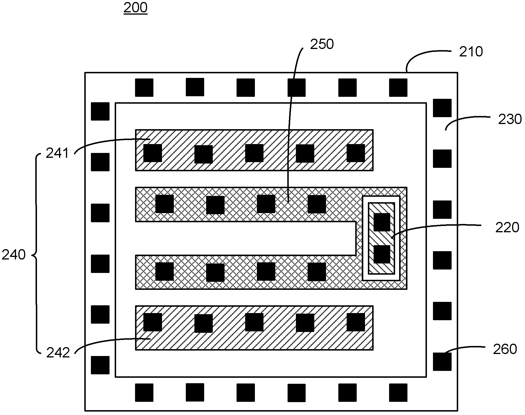
[0035] According to the first embodiment of the present invention, such as figure 2 As shown, the P-type doped region 240 includes a first P-type doped region 241 and a second P-type doped region 242 . The N-type doped region 250 is located between the first P-type doped region 241 and the second P-type doped region 242 . According to the requirements of the process size of the sample to be tested, the width of the N-type doped region 250 can be set, and then the N-type doped region 250 with the width can be tested for doping loss by means of a detection device. If there is a doping loss, the width of the N-type doped region 250 is increased.

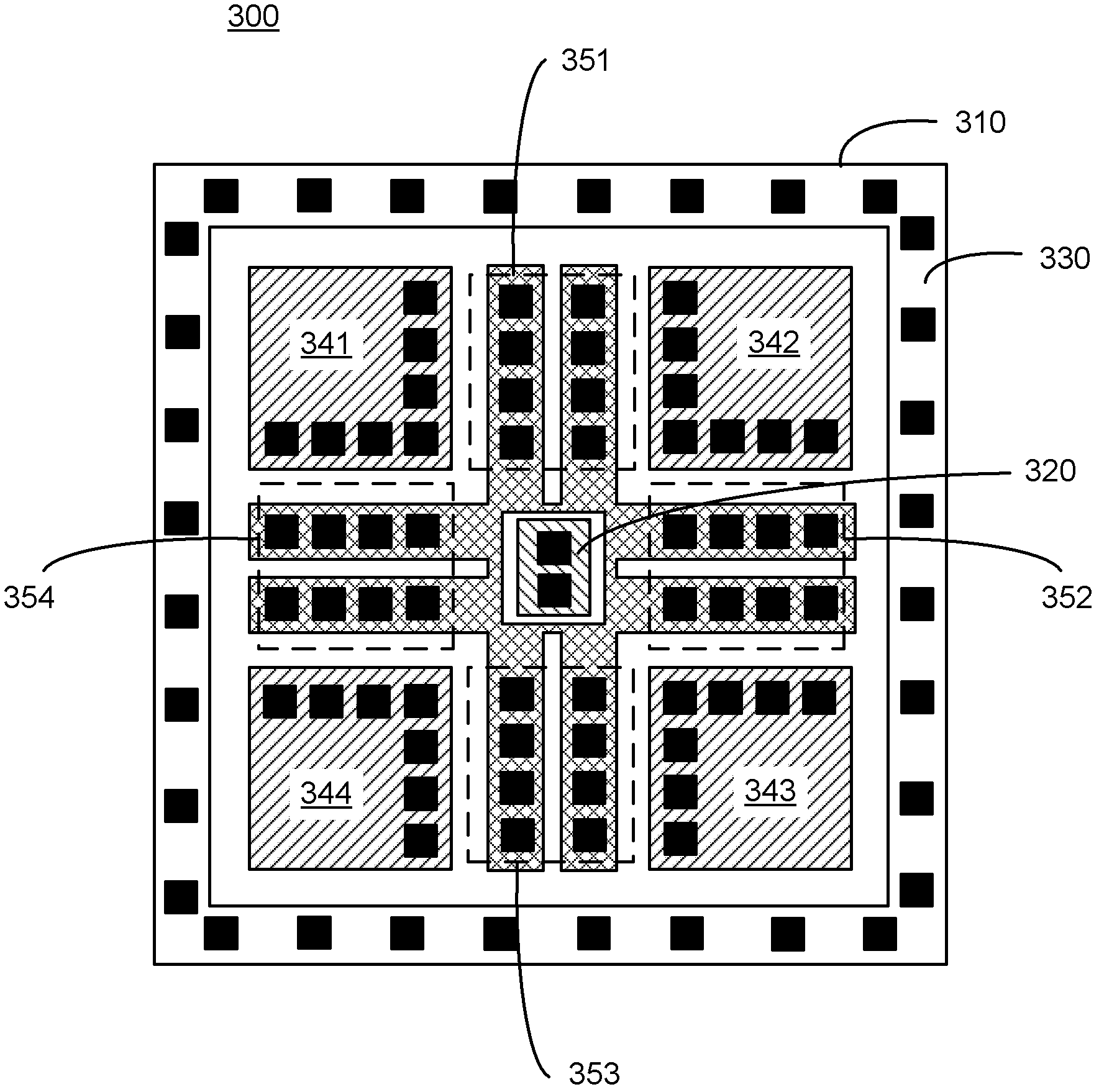
[0036] According to the second embodiment of the present invention, such as image 3 As shown, the P-type doped region includes a first P-type doped region 341 , a second P-type doped region 342 , a third P-type doped region 343 and a fourth P-type doped region 344 . The N-type doped region includes a first N-type doped region 351, ...


PUM


Abstract

The invention discloses a test component used in a complementary metal-oxide-semiconductor transistor (CMOS) component and a manufacture method and a using method thereof. The test component used in the CMOS component comprises a semiconductor substrate, an N-type well region, a P-type well region, a P-type doped area, an N-type doped area and contact holes, wherein the semiconductor substrate comprises a test area, the N-type well region and the P-type well region are arranged in the test area of the semiconductor substrate, the P-type doped area is arranged in the N-type well region, the N-type doped area is arranged in the P-type well region and has a preset width, and the contact holes are formed in the N-type well region, the P-type well region, the P-type doped area and the N-type doped area and are used for enabling the N-type well region, the P-type well region, the P-type doped area and the N-type doped area to be communicated with other components. According to the test component used in the CMOS component, doping loss exists in the CMOS component can be found in time, process windows are confirmed, and influence to the manufacture of follow-up wafers is avoided, and thus yield is improved, and cost is reduced.

Description

technical field [0001] The invention relates to a semiconductor manufacturing process, in particular to a testing device for a CMOS device, a manufacturing method and a using method thereof. Background technique [0002] figure 1 For the cross-sectional view of the process of forming a CMOS device in the prior art, refer to the following figure 1 To illustrate the fabrication process of CMOS devices. The manufacturing process of the CMOS device includes the following steps: forming an N-type well region (N + ) and the P-type well region (P + ), wherein a shallow trench isolation region 101 has been formed in the semiconductor substrate 100; a photoresist layer 102 is covered on the N-type well region and an N-type doping process is performed to form an N-type doped region in the P-type well region (not shown) forming the N-type doped region of the NMOS device; covering the photoresist layer on the P-type well region and performing a P-type doping process to form the P-ty...

Claims


Application Information

Patent Timeline
Patent Type & Authority Applications(China)
IPC IPC(8): H01L23/544H01L21/02G01R31/26H01L21/66
Inventor 王喆张喆
Owner SEMICON MFG INT (SHANGHAI) CORP
Why Eureka
Try Eureka