Solar cell electrode printing mask plate and manufacturing method thereof
A solar cell and reticle technology, applied in printing, printing machine, printing plate preparation, etc., can solve problems such as limiting the conversion rate of solar cells, and achieve the effects of improving photoelectric conversion efficiency, reducing losses, and uniformity
- Summary
- Abstract
- Description
- Claims
- Application Information
AI Technical Summary
Problems solved by technology
Method used
Image
Examples
Embodiment 1
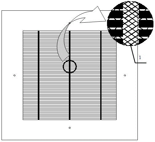
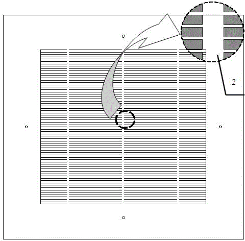
[0042] Figure 7 Shown is a flow chart of an embodiment of the present invention, the mask involved is a two-layer structure, and the specific scheme is as follows:
[0043] a. Pre-treat the stainless steel mandrel to make the surface of the mandrel clean and smooth.
[0044] b. Coat a layer of photosensitive film evenly on the stainless steel mandrel; transfer the first layer pattern of the electrode mask plate of the solar cell to the photosensitive dry film through an exposure machine; perform a series of processes such as developing, cleaning and drying after exposure, and unpainted The dry film at the exposed area is cleaned and dissolved, leaving the solar cell electrode mask pattern. The first thin grid line and the main grid line of the solar cell electrode mask are connected by bridges between the grid lines. Corresponding; put the mandrel with the pattern made into the electroforming solution for electrodeposition molding, and take out the mandrel with a layer of el...
Embodiment 2
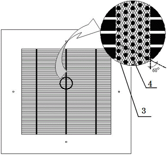
[0049] On the main grid line of the mask plate, an array point that is impenetrable to conductive silver paste is arranged, and the graphic shape of the array point can be any shape, such as a circle, a rhombus, a rectangle, a square, a triangle, a polygon, etc., preferably a circle; When the shape of the array point is circular, the diameter of the circle is 50um-1mm; when the shape of the array point is rectangular, the side length of the circle is 50um-1mm; when the shape of the array point is triangular, The side length of the triangle is 50um-1mm; the distance between the centers of the array points is 50um-1mm; the row (or column) where the array points are located is parallel to, perpendicular to, or at a certain angle to the main grid line. image 3 It is a mask plate with array points; 3 is an enlarged schematic diagram of the main grid line and the fine grid line, the graphic shape of the array point 4 is circular, the diameter is 50um, and the distance between the ce...
Embodiment 3
[0051] Figure 4 Shown is a schematic diagram of a mask with side holes. The surrounding edges of the mask plate are provided with side holes arranged according to certain rules; the side holes of the mask plate can be in any shape, preferably circular; there are two rows of side holes parallel to the sides near each side of the mask plate, and each row Scattered at equal intervals; the side holes are used to fix the mask on the frame with glue or on the frame through a silk screen.
PUM
 Abstract
Description
Claims
Application Information


