Thermal field of monocrystalline silicon manufacturing device

A technology for manufacturing devices and single crystal silicon, which is applied in the directions of single crystal growth, single crystal growth, crystal growth, etc., can solve the problems of supercooling of components and difficult to increase temperature gradient, and achieve the effect of reducing the scouring effect

Inactive Publication Date: 2013-06-26
HUIXIN PHOTOELECTRIC TECH JIANGSU
View PDF0 Cites 1 Cited by
  • Summary
  • Abstract
  • Description
  • Claims
  • Application Information

AI Technical Summary

Problems solved by technology

[0003] Aiming at the deficiencies of the prior art, the present invention proposes a method that can solve the problems that the temperature gradient near the growth interface is diff

Method used


Image

  • Thermal field of monocrystalline silicon manufacturing device
  • Thermal field of monocrystalline silicon manufacturing device

Examples


Example Embodiment

[0012] The present invention will be further described below according to the accompanying drawings and in conjunction with the embodiments.

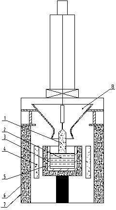
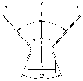
[0013] like figure 1 The thermal field of the monocrystalline silicon manufacturing device shown includes a furnace wall 7, a quartz crucible 3, a graphite crucible 5, a graphite heater 4, and a graphite spacer 6. The quartz crucible 3 is placed in the graphite crucible 5, and the graphite heater 4 is set Around the graphite crucible 5; the graphite spacer 6 is set on the inner wall of the furnace wall 7, and the graphite heater 4 is surrounded in the inner space; the rod-shaped single crystal silicon 1 is pulled out from the molten silicon 2 in the quartz crucible 3. The top of the quartz crucible 3 is provided with a conical gas guide hood 8. In the present invention, the gas guide hood 8 is as figure 2 As shown, it is made of high-purity graphite and is a combination of upper and lower cones. The small ends of the upper and low...


PUM


Abstract

The invention discloses a thermal field of a monocrystalline silicon manufacturing device, which comprises a furnace wall, a quartz crucible, a graphite crucible, a graphite heater, a graphite spacer bush. The quartz crucible is disposed inside the graphite crucible. The graphite heater is disposed around the graphite crucible. The graphite spacer bush is sleeved to the inner side of the furnace wall and encloses thee graphite heater inside an inner space of the graphite spacer. A conical guide hood is arranged above the quartz crucible. The thermal field of the monocrystalline silicon manufacturing device is characterized in that the guide hood is formed by an upper cone and a lower cone, and the upper cone and the lower cone are hermetically connected at the lower ends and are smoothly connected via an arc face. The hole diameter D1 of the large end of the upper cone is larger than the hole diameter D3 of the larger end of the lower cone. The guide hood formed by the upper cone and the lower cone helps to increase longitudinal temperature gradient nearby a solid-liquid interface and maintain not fast cooling speed of crystal nearby a growth interface, and in addition, scouring action of protective gases on the growth interface can be evidently reduced.

Description

technical field [0001] The invention relates to a thermal field of a monocrystalline silicon manufacturing device, in particular, the invention relates to a thermal field of a monocrystalline silicon device manufactured by a Czochralski method. Background technique [0002] In a single crystal silicon manufacturing device that uses the Czochralski method to manufacture single crystal silicon, the thermal field plays a crucial role in the growth of single crystal silicon. The thermal field of the existing monocrystalline silicon device includes a furnace wall, a quartz crucible, a graphite crucible, a graphite heater, and a graphite spacer. The quartz crucible is placed in the graphite crucible, and the graphite heater is arranged around the graphite crucible; The inner wall of the wall encloses the graphite heater in its inner space. The thermal field of the single crystal silicon device in the prior art can be used to grow lightly doped single crystal silicon, but it canno...

Claims


Application Information

Patent Timeline
IPC IPC(8): C30B15/14C30B29/06
Inventor 袁文宝
Owner HUIXIN PHOTOELECTRIC TECH JIANGSU
Why Eureka
Try Eureka