

Circuit board, display module, and electronic apparatus
A technology for display modules and circuit boards, applied in the direction of circuits, printed circuit components, structural connections of printed circuits, etc., can solve problems such as joint failure and displacement, and achieve the effects of suppressing damage, good wiring connections, and increasing production.
- Summary
- Abstract
- Description
- Claims
- Application Information
AI Technical Summary
Problems solved by technology
Method used
Image

Examples
Embodiment approach
[0042] [structure]
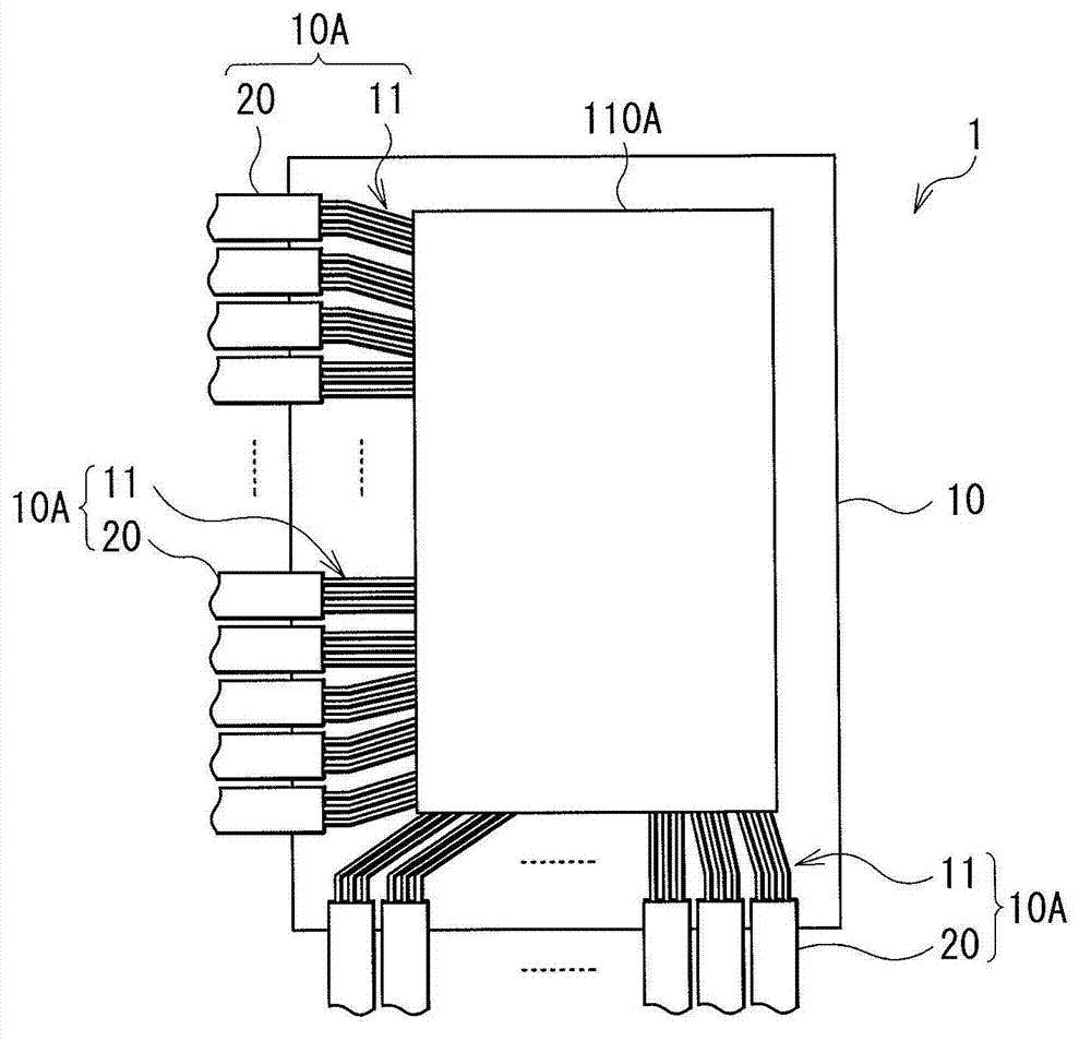
[0043] figure 1 The configuration of a display module (display module 1 ) according to an embodiment of the present disclosure is schematically shown. The display module 1 is configured by bonding (connecting, bonding) a plurality of flexible printed circuit boards (hereinafter referred to as FPCs) 20 on a part of the substrate 10 . Note that the substrate 10 corresponds to a specific example of the “first substrate” of the present disclosure, and the FPC 20 corresponds to a specific example of the “second substrate” of the present disclosure. In addition, the configuration (substrate 10 , device portion, and bonding portion 10A) of the display module 1 corresponds to a specific example of a “circuit board” of the present disclosure, except for a later-described display portion 110A.
[0044] Made of such as polyimide (PI), polyethylene terephthalate (PET), polyethersulfone (PES), polyethylene naphthalate (PEN), polycarbonate (PC) and liquid crystal A f...
Deformed example 1
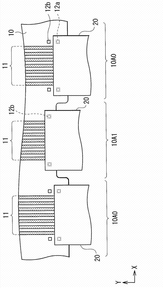
[0093] In this embodiment, although the case where the slit 13 is formed for each bonding portion 10A1 has been described, similarly to Modification 1, the slit 13 may be formed across a plurality of bonding portions 10A1. For example, if Figure 12As shown, one (common) cutout 13d may be formed for two adjacent joint portions 10A1. In this case, when the connection failure X occurs in the adjacent pair of wiring layers 11 and FPC 20 at the time of the first FPC bonding, the cutout 13 d is formed to integrally cut off the two pairs of wiring layers 11 and FPC 20 . Then, FPC bonding is performed again for each wiring layer 11 to realize repair mounting as described above. This is especially effective when the pitch between adjacent wiring layers 11 is narrow.
[0094] Incidentally, although the case where the slit 13d is formed across adjacent two joint portions 10A1 has been described here, if connection failure X or other conditions occur across three or more pairs arranged...
Deformed example 2
[0096] Also, in this embodiment, the cutout 13 having a rectangular shape and also having curved corners (no curved portion) has been exemplified. Alternatively, the cutouts of the present disclosure may have other shapes.
[0097] For example, if Figure 13A Of the cutouts 13a shown, only the corner a1 on the inside of the rectangular shape has a curved shape, and the corner a2 on the outside may have a curved shape (for example, a right-angled shape). In addition, if Figure 13B The shape of the cutout 13b shown in the XY plane may be a trapezoid with the inner side b1 of the substrate 10 as the upper base. In addition, if Figure 13C A rectangular shape in which the cutout 13c is shown, and the corners a1 and a2 are bent at right angles is also usable. However, from the viewpoint of impact resistance and mold management as described above, it is desirable that the slit has a shape without a bent portion.
PUM
| Property | Measurement | Unit |
|---|---|---|
| Thickness | aaaaa | aaaaa |
| Thickness | aaaaa | aaaaa |
Abstract
Description
Claims
Application Information