Semiconductor failure analysis structure, forming method of semiconductor failure analysis structure and failure time detection method thereof

A failure analysis and failure time technology, which is applied in the direction of single semiconductor device testing, semiconductor devices, semiconductor/solid-state device components, etc., can solve problems such as difficult identification of test equipment, small voltage between test pads, and difficulty in detecting electromigration

Active Publication Date: 2013-07-03
SEMICON MFG INT (SHANGHAI) CORP
View PDF6 Cites 14 Cited by
  • Summary
  • Abstract
  • Description
  • Claims
  • Application Information

AI Technical Summary

Problems solved by technology

[0007] As the development direction of semiconductor technology is integration and miniaturization, it can be proved by experiments that the miniaturization of semiconductor devices can improve its life and speed. The value is also getting smaller and smaller, resulting in a smaller and smaller

Method used


Image

  • Semiconductor failure analysis structure, forming method of semiconductor failure analysis structure and failure time detection method thereof
  • Semiconductor failure analysis structure, forming method of semiconductor failure analysis structure and failure time detection method thereof
  • Semiconductor failure analysis structure, forming method of semiconductor failure analysis structure and failure time detection method thereof

Examples


specific Embodiment 1

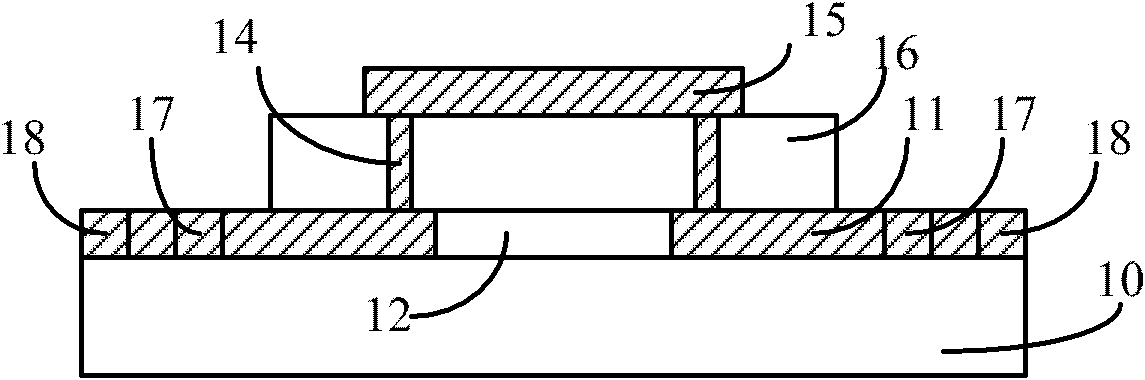
[0094] Please refer to figure 2 , a method for forming a semiconductor failure analysis structure, comprising the following steps:

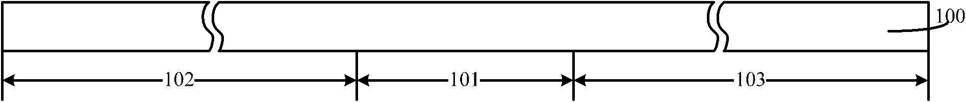
[0095] Step S101, providing a semiconductor substrate, the semiconductor substrate has a region to be tested, a first series region and a second series region located on both sides of the region to be tested;

[0096] Step S102, forming a metal layer to be tested on the surface of the semiconductor substrate to be tested, and forming several discrete short metal layers on the surface of the first serial region and the second serial region;

[0097] Step S103, forming an insulating layer between the metal layer to be tested and several discrete short metal layers;

[0098] Step S104, forming an interlayer dielectric layer on the surface of the metal layer to be tested, several discrete short metal layers, and the insulating layer;

[0099] Step S105, forming a first conductive plug, a second conductive plug, and a third conductive plug through ...

specific Embodiment 2

[0125] Please refer to Figure 7 , a method for forming a semiconductor failure analysis structure, comprising the following steps:

[0126] Step S201, providing a semiconductor substrate, the semiconductor substrate has a region to be tested, a first series region and a second series region located on both sides of the region to be tested;

[0127] Step S202, forming a first metal layer, a second metal layer and a metal interconnection layer on the surface of the semiconductor substrate, the first metal layer straddles the region to be tested and the first series region, and the second metal layer straddles the region to be tested The measurement area and the second series area, the metal interconnection layer is in the first series area and the second series area;

[0128] Step S203, forming an insulating layer between the first metal layer, the second metal layer and the metal interconnection layer;

[0129] Step S204, forming an interlayer dielectric layer on the surface...


PUM

PropertyMeasurementUnit
Resistanceaaaaaaaaaa
Lengthaaaaaaaaaa
Total lengthaaaaaaaaaa

Abstract

The invention provides a semiconductor failure analysis structure, a forming method of the semiconductor failure analysis structure and a failure time detection method thereof. The semiconductor failure analysis structure comprises a semiconductor substrate, a metal layer to be tested, a first metal layer, a second metal layer, a first conductive plug, a plurality of first resistance metal layers, a plurality of second resistance metal layers, a plurality of second conductive plugs and a plurality of third conductive metal layers. The semiconductor substrate is provided with an area to be tested, a first serial area and a second serial area. The metal layer to be tested, the first metal layer and the second metal layer are placed on the semiconductor substrate. The first conductive plug placed in an interlayer dielectric layer enables the first metal layer, the second metal layer and the metal layer to be tested to be connected in series. The plurality of first resistance metal layers are arranged in the first serial area. The plurality of second resistance metal layers are arranged in the second serial area. The plurality of second conductive plugs are placed in the interlayer dielectric layer of the first serial area. The plurality of third conductive metal layers are arranged in the interlayer dielectric layer of the second serial area. The first conductive plug, the second conductive plugs and the third conductive plugs enable the metal layer to be tested, the first metal layer, the second metal layer, the plurality of first resistance metal layers and the plurality of second resistance metal layers to be sequentially connected in series.

Description

technical field [0001] The invention relates to a semiconductor manufacturing process, in particular to a semiconductor failure detection structure and a forming method, and a method for detecting failure time. Background technique [0002] The development requirements of high complexity and high integration of large-scale integrated circuits make semiconductor devices must have higher reliability. However, currently there are many reasons affecting the reliability of semiconductor devices, among which electro-migration (Electro-Migration; EM for short) phenomenon is one of the reasons leading to failure of semiconductor devices. Specifically, electromigration can lead to an open circuit or a short circuit inside a semiconductor device, increasing the leakage of the device and causing it to fail. The cause of electromigration is the movement of metal atoms. When the current density in the metal interconnection line is high, the electrons move from the cathode to the anode a...

Claims


Application Information

Patent Timeline
IPC IPC(8): H01L23/544G01R31/26
Inventor 陈芳甘正浩
Owner SEMICON MFG INT (SHANGHAI) CORP
Why Eureka
Try Eureka