Complementary Metal-Oxide-Semiconductor Transistor (CMOS) image sensor and production method thereof

An image sensor and area technology, applied in the field of CMOS image sensor and its preparation, can solve the problems of limiting the detection limit and dynamic range of image sensors, and achieve the effects of improving efficiency, reducing image delay, and increasing transmission speed

Inactive Publication Date: 2013-07-17
SHANGHAI HUALI MICROELECTRONICS CORP
View PDF4 Cites 2 Cited by
  • Summary
  • Abstract
  • Description
  • Claims
  • Application Information

AI Technical Summary

Problems solved by technology

[0008] The present invention is aimed at the prior art, the dark current in the traditional 3T structure limits the detection limit and dynamic range of the image sensor; in the 4T structure, the electrons in the photodiode cannot be completely transferred to the floating node caused by the junction distribution problem in the pinning diode defects such as image delay to provide a CMOS image sensor
[0009] Another object of the present invention is to aim at the prior art, the dark current in the traditional 3T structure limits the detection limit and the dynamic range of the image sensor; Defects such as image delays transferred to floating nodes provide a fabrication method for CMOS image sensors

Method used


Image

  • Complementary Metal-Oxide-Semiconductor Transistor (CMOS) image sensor and production method thereof
  • Complementary Metal-Oxide-Semiconductor Transistor (CMOS) image sensor and production method thereof
  • Complementary Metal-Oxide-Semiconductor Transistor (CMOS) image sensor and production method thereof

Examples


Embodiment Construction

[0027] In order to illustrate the technical content, structural features, achieved goals and effects of the present invention in detail, the following will be described in detail in conjunction with the embodiments and accompanying drawings.

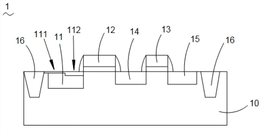
[0028] see figure 1 , figure 1 Shown is a schematic structural diagram of the CMOS image sensor of the present invention. The shown CMOS image sensor 1 includes a photodiode 11, a transfer transistor 12, a reset transistor 13, a first floating node 14, a second floating node 15 arranged in the semiconductor substrate 10, and an isolation structure for electrical isolation of devices 16, wherein the photodiode 11 has at least two first regions 111 and second regions 112 with different indium doping concentrations, and the indium doping concentration of the first region 111 at the far end of the transfer transistor 12 is lower than that at the Indium doping concentration of the second region 112 near the end of the transfer transistor 12...


PUM


Abstract

A Complementary Metal-Oxide-Semiconductor Transistor (CMOS) image sensor comprises a photodiode, a shifting transistor, a reset transistor, a first floating node and a second floating node which are arranged in a semiconductor substrate and an isolation structure used for device electric isolation. The photodiode is provided with at least two zones, namely a first zone and a second zone, having different indium doping concentrations, and the indium doping concentration of the first zone located at the far end of the shifting transistor is smaller than that of the second zone located at the near end of the shifting transistor. At least two-time ion injection at different angles is adopted, and an internal electric field E pointing from the second zone to the first zone is formed in the photodiode through the shielding effect of ion injection, so that photoelectron transmission speed is improved, the number of photoelectrons detained in the photodiode is reduced, photoelectron collection efficiency of the photodiode is improved, and image delay or information losing is reduced.

Description

technical field [0001] The invention relates to the technical field of semiconductors, in particular to a CMOS image sensor and a preparation method thereof. Background technique [0002] CMOS image sensor (CMOS Image Sensor, CIS) has obvious advantages over existing charge coupled device (Charge Coupled Device, CCD) by virtue of its manufacturing process and general integrated circuit standard process flow compatibility. CMOS image sensors do not have the inherent defects of large size, high power consumption, and poor compatibility in CCD technology. Instead, they can make full use of existing processes and equipment, and integrate with associated processing circuits, with a high degree of system integration. In addition, compared with CCDs, CMOS image sensors have the advantages of small size, low power consumption, high speed, and low cost, and have been widely used in photography and camera products. [0003] Traditional active pixels use photodiodes as image sensing d...

Claims


Application Information

Patent Timeline
Patent Type & Authority Applications(China)
IPC IPC(8): H01L27/146
Inventor 田志江润峰
Owner SHANGHAI HUALI MICROELECTRONICS CORP
Why Eureka
Try Eureka