

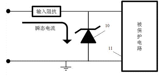
Low capacitance super-deep groove transient voltage restraining diode structure
A transient voltage suppression, deep trench technology, applied in circuits, electrical components, semiconductor devices, etc., to achieve the effect of increasing junction area, high resistance to high surge current, and reducing size
- Summary
- Abstract
- Description
- Claims
- Application Information
AI Technical Summary
Problems solved by technology
Method used
Image

Examples
Embodiment Construction
[0019] The preferred embodiments of the present invention will be described in detail below in conjunction with the accompanying drawings, so that the advantages and features of the present invention can be more easily understood by those skilled in the art, so as to define the protection scope of the present invention more clearly.
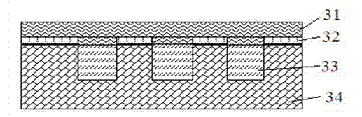
[0020] The present invention uses an innovative ultra-deep trench (greater than 10 μm), N-type doped polysilicon (poly-Si) filling and near intrinsic lightly doped N-type epitaxial (near intrinsic N-Epi) structure to manufacture small-scale , Low capacitance TVS diode devices.
[0021] see Figure 4 , Figure 4 It is a structural schematic diagram of a low-capacitance ultra-deep trench TVS diode structure. The low-capacitance ultra-deep trench TVS diode structure includes a heavily doped P-type substrate 41, a heavily doped N-type epitaxial layer 42, a lightly doped N-type epitaxial layer 43, silicon dioxide (SiO 2 ) layer 44 , an interlayer i...
PUM
| Property | Measurement | Unit |
|---|---|---|
| Depth | aaaaa | aaaaa |
| Resistivity | aaaaa | aaaaa |
| Resistivity | aaaaa | aaaaa |
Abstract
Description
Claims
Application Information