
Novel light-operated light emitting diode based on nano material

A light-emitting diode, a new type of technology, applied in the direction of electrical components, circuits, semiconductor devices, etc., can solve the problems of reducing data storage density and accuracy, low thermal stability, easy aging, etc., and achieve the effect of improving the ON/OFF ratio

Inactive Publication Date: 2013-08-14
SUZHOU RUISHENG SOLAR ENERGY TECH
View PDF5 Cites 11 Cited by
  • Summary
  • Abstract
  • Description
  • Claims
  • Application Information

AI Technical Summary

Problems solved by technology

However, due to the low thermal stability of the organic material itself, it is easy to age under the condition of water and oxygen, so its practical application is very limited.
In addition, the spectrum of organic light-emitting materials is relatively wide, and the half-peak width is generally about 50-100 nanometers, which reduces the density and accuracy of data storage.

Method used


Image

  • Novel light-operated light emitting diode based on nano material
  • Novel light-operated light emitting diode based on nano material

Examples


Embodiment Construction

[0019] Preferred embodiments of the present invention will be described in detail below in conjunction with the accompanying drawings.

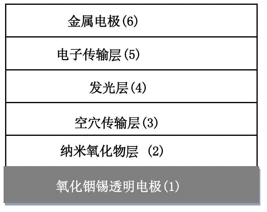
[0020] Such as figure 1 Shown is a schematic diagram of the structure of a light-controlled light-emitting diode. The device includes: a transparent conductive substrate 1; a photosensitive nanomaterial layer 2, the conductive performance of which is significantly improved after the active layer 2 is irradiated by a specific light source; a hole transport layer 3, which is made on a photosensitive nano Materials on the active layer 2; the light emitting layer 4; the electron transport layer 5; and the metal electrode 6.

[0021] The conductive substrate 1 is an oxide transparent conductive film, usually an indium tin oxide film or a zinc oxide film doped with aluminum, gallium or cadmium, with a thickness between 20-2000 nanometers. On the conductive substrate 1 is a nano-photosensitive active layer 2 prepared by solution method (generally ...


PUM

PropertyMeasurementUnit
Thicknessaaaaaaaaaa
Thicknessaaaaaaaaaa
Thicknessaaaaaaaaaa

Abstract

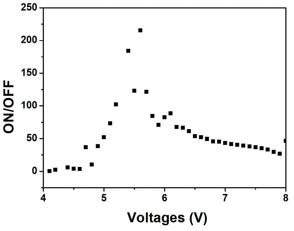
The invention discloses a novel light-operated light emitting diode based on nano material. The novel light-operated light emitting diode comprises a transparent conductive substrate, a nano oxide layer, a hole transmission layer, a light emitting layer, an electron transmission layer and a metal electrode, wherein the conduction property of the nano oxide can be changed upon illumination. The light-operated light emitting diode can be prepared through a solution method, so as to have the advantages of low manufacture cost and convenience for large scale production; before illumination, the high ionization energy of the nano oxide prevent injection of holes, so that the brightness of the light emitting diode is low; after illumination, due to the photodoping effect of the nano oxide layer, the conduction property of the nano oxide layer is greatly increased, so that the holes go through the highly conductive nano oxide and are injected into illumination layer, the illumination brightness of the device is greatly increased, the light-operation of the light emitting diode is realized, and the ON / OFF ratio of the brightness and the currency density before and after the illumination are 200 and 10,000 respectively.

Description

technical field [0001] The invention belongs to the field of optoelectronic devices, and relates to a novel light-controlled light-emitting diode based on nanometer materials and a preparation method of the light-emitting diode. Background technique [0002] With the continuous progress of information technology, people pay more and more attention to new intelligent devices. Among them, light-controlled light-emitting diodes can adjust the ON / OFF state through light, and are widely used in different fields such as remote control, data storage, and photosensitive sensors. In recent years, researchers have developed photo-controllable light-emitting diodes based on DTE. Using the molecular configuration and carrier transport ability of this organic material under different illuminations, the photo-control effect has been realized. The ON / The OFF ratios are all above 1000. However, due to the low thermal stability of the organic material itself, it is easy to age under the c...

Claims


Application Information

Patent Timeline
IPC IPC(8): H01L33/14H01L33/26H01L33/00
Inventor 钱磊章婷刘德昂
Owner SUZHOU RUISHENG SOLAR ENERGY TECH
Learn More