Calcium-doped zinc oxide thin film transistor and manufacturing method thereof

A technology of thin-film transistors and zinc oxide nanocrystals, which is applied in the direction of transistors, semiconductor/solid-state device manufacturing, semiconductor devices, etc., can solve the problems of high manufacturing cost, environmental protection, and difficult application, and achieve low manufacturing cost, simple steps, and uniformity good sex effect

Inactive Publication Date: 2015-07-08
PEKING UNIV
View PDF3 Cites 0 Cited by
  • Summary
  • Abstract
  • Description
  • Claims
  • Application Information

AI Technical Summary

Problems solved by technology

However, In is a rare and toxic element, and the use of In-doped materials is costly and environmentally unfriendly to manufacture, making it difficult to be widely used in large-scale production.

Method used


Image

  • Calcium-doped zinc oxide thin film transistor and manufacturing method thereof
  • Calcium-doped zinc oxide thin film transistor and manufacturing method thereof
  • Calcium-doped zinc oxide thin film transistor and manufacturing method thereof

Examples


Embodiment Construction

[0029] The present invention will be further described below by example. It should be noted that the purpose of the disclosed examples is to help further understand the present invention, but those skilled in the art can understand that various replacements and modifications are possible without departing from the scope of the present invention and the spirit of the appended claims. Therefore, the present invention should not be limited to the content disclosed in the examples, and the protection scope of the present invention is subject to the scope defined in the claims.

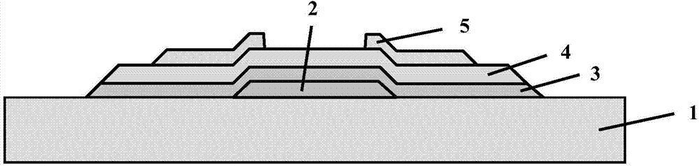
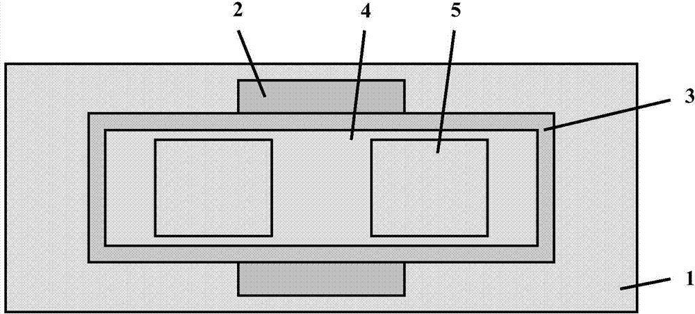
[0030] The thin film transistor of the present invention is formed on glass or plastic substrate 1, as figure 1 with figure 2 shown. The thin film transistor includes a gate electrode 2 , a gate dielectric layer 3 , a semiconductor conductive channel layer 4 , and source and drain terminal electrodes 5 . The gate electrode 2 is located on the glass or plastic substrate 1, the gate dielectric layer 3 is...


PUM

PropertyMeasurementUnit
particle sizeaaaaaaaaaa

Abstract

The invention provides a thin film transistor and a manufacturing method thereof and belongs to the fields of the semiconductor industry and panel display. The core is that calcium-doped zinc oxide semiconductor materials are adopted and made into a conducting channel layer of the thin film transistor, the size of manufactured semiconductor thin film grains is smaller than 20 nanometers, and the semiconductor thin film grains are uniformly distributed and belong to nanocrystalline oxide semiconductors. The process method has the advantages that steps are simple, manufacturing cost is low, uniformity is good, the method is used for low-temperature processes and has an active effect of improving the performance of a thin film transistor device, the performance in the aspects of the mobility, switching ratio, threshold voltage, subthreshold swing and the like of the device is improved, and the method is suitable for transparent display and flexible display technologies.

Description

technical field [0001] The invention relates to a method for preparing a thin film transistor on a glass substrate or a plastic substrate, and belongs to the field of semiconductor industry and flat panel display. Background technique [0002] In the information age, display technology occupies an important position, and the increasing development of display technology has brought people a more colorful visual experience. Today's flat panel display technologies include AMLCD (Liquid Crystal Display), AMOLED (Organic Light Emitting Diode Display), flexible display, transparent display, etc. With the continuous development of display technology, the brightness, viewing angle, full color and other aspects of flat panel display (FPD) have been improved. [0003] Transparent electronic display is a frontier topic in the field of display today. Therefore, the exploration and research on transparent oxide semiconductor thin films has become the key. Transparent conductive oxide m...

Claims


Application Information

Patent Timeline
Patent Type & Authority Applications(China)
IPC IPC(8): H01L29/786H01L29/227H01L21/34
CPCH01L29/786H01L29/1033H01L29/227H01L29/66772H01L29/7869
Inventor 韩德栋郁文王漪石盼丛瑛瑛张翼董俊辰周晓梁黄伶灵张盛东刘力锋刘晓彦康晋锋
Owner PEKING UNIV
Why Eureka
Try Eureka