Preparation method for zinc oxide thin-film transistor

A technology of thin film transistor and zinc oxide, applied in semiconductor/solid-state device manufacturing, semiconductor devices, electrical components, etc., can solve the problems of high manufacturing cost, rare content, unenvironmental protection, etc., and achieve low manufacturing cost, improved performance, uniformity, etc. Good results

Inactive Publication Date: 2014-10-22
PEKING UNIV
View PDF3 Cites 0 Cited by
  • Summary
  • Abstract
  • Description
  • Claims
  • Application Information

AI Technical Summary

Problems solved by technology

Among them, IGZO is considered to be the most promising transparent semiconductor material. However, because In in the material is a rare element, the content on the earth is scarce, In and Ga elements are poisonous, the manufacturing cost is high and it is not environmentally friendly.
Zinc-nickel oxide (NZO) has not yet been studied, and Ni is common and non-toxic, environmentally friendly and healthy, so it is of great scientific value and practical significance to study zinc-nickel oxide as a transparent conductive material and semiconductor material

Method used


Image

  • Preparation method for zinc oxide thin-film transistor
  • Preparation method for zinc oxide thin-film transistor
  • Preparation method for zinc oxide thin-film transistor

Examples


Embodiment Construction

[0028] The present invention will be further described below by specific examples.

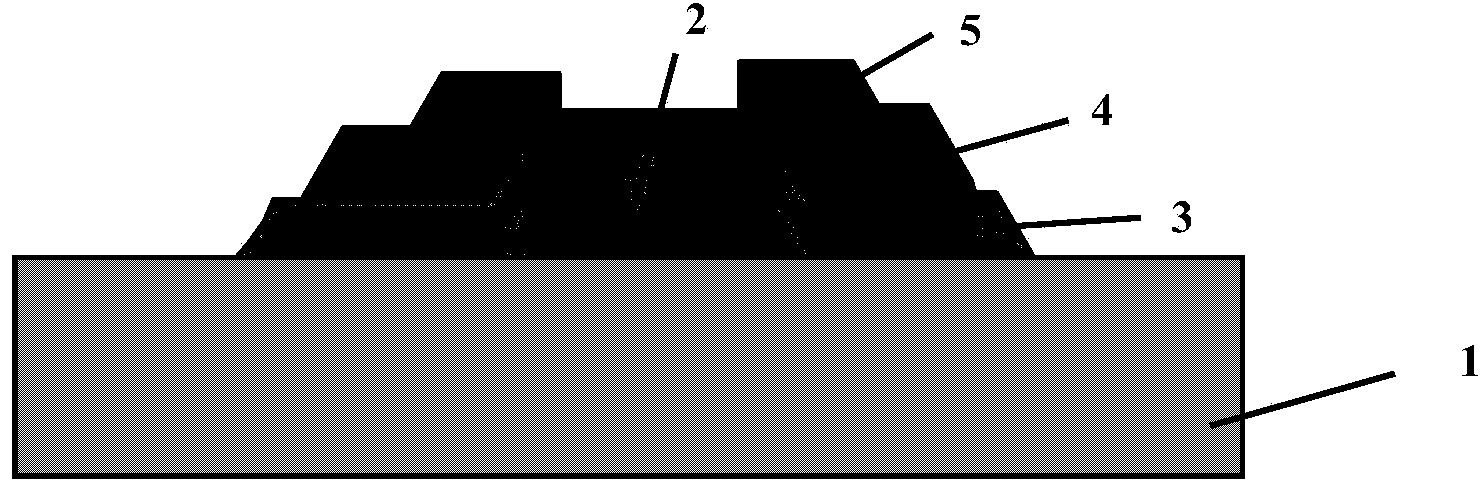
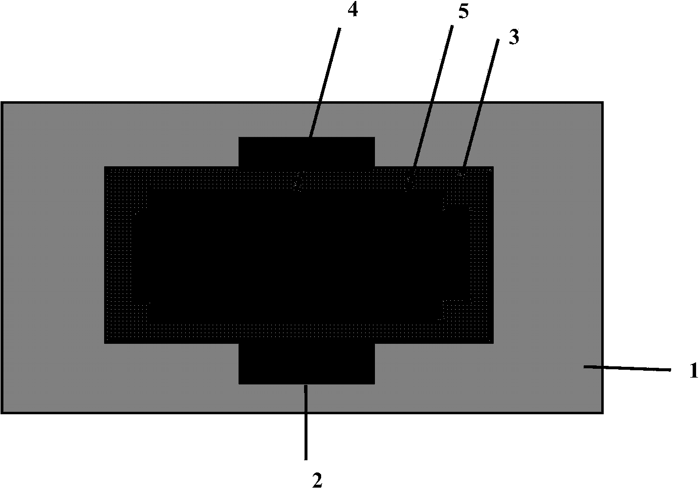
[0029] The concrete example of the manufacturing method of the thin film transistor of the present invention is by Figure 3(a) to Figure 3(e) shown, including the following steps:

[0030] As shown in FIG. 3( a ), the substrate is a transparent glass or plastic substrate substrate 1 .

[0031] As shown in FIG. 3( b ), a 30-150 nanometer thick ITO conductive film is grown on the substrate 1 by magnetron sputtering technology, and then the gate electrode is etched by photolithography.

[0032] As shown in FIG. 3( c ), a silicon dioxide insulating layer with a thickness of 50-250 nanometers is grown by PECVD, and then photolithography is used to form a gate dielectric.

[0033] As shown in FIG. 3( d ), a nickel-doped zinc oxide semiconductor material channel layer is grown by a sputtering process. The target used for sputtering is nickel-doped zinc oxide ceramic target, the content of nickel ...


PUM


Abstract

The invention discloses a preparation method for a zinc oxide thin-film transistor and belongs to the semiconductor industry and panel display field. The preparation method uses a sputtering technology to grow a nickel-doped zinc oxide semiconductor material layer which servers as a conducting channel layer of the thin-film transistor, and the switch ratio, sub-threshold swing, threshold voltage, mobility ratio and the like of the thin-film transistor can be improved through regulating ingredients of nickel-doped zinc oxide target and controlling the sputtering oxygen partial pressure. The preparation method for the zinc oxide thin-film transistor has advantages that the manufacturing cost is low, the low-temperature technique is suitable for transparent display and flexible display technologies, and the like.

Description

technical field [0001] The invention relates to a method for preparing a thin film transistor on a glass substrate or a plastic substrate, and belongs to the field of semiconductor industry and flat panel display. Background technique [0002] With the advent of the information age, display devices are accelerating towards flat panelization and energy saving. Among them, active array drive display devices with thin-film transistors (TFT) as switching elements have become the best among many flat panel display technologies. TFT is a field-effect semiconductor device, including several important components such as substrate, semiconductor channel layer, insulating layer, gate and source-drain electrodes, among which the semiconductor channel layer is crucial to device performance and manufacturing process influences. In the last decade or so, liquid crystal display devices using silicon (amorphous silicon and polysilicon) TFTs as drive units have developed rapidly due to thei...

Claims


Application Information

Patent Timeline
Patent Type & Authority Applications(China)
IPC IPC(8): H01L21/34H01L21/203
CPCH01L29/66742H01L29/7869
Inventor 韩德栋黄伶灵陈卓发丛瑛瑛赵楠楠吴静赵飞龙董俊辰王漪刘力锋张盛东刘晓彦康晋锋
Owner PEKING UNIV
Why Eureka
Try Eureka