Tin ball production method and equipment for semiconductor packaging

A solder ball and equipment technology, applied in the field of solder ball manufacturing and equipment for semiconductor packaging, can solve the problems of high cost of production equipment, uneven thickness of tin wires, affecting the size of solder balls, etc., and achieves convenient operation and high yield. , the effect of increasing productivity

Active Publication Date: 2013-08-21
江苏矽智半导体科技有限公司
View PDF4 Cites 1 Cited by
  • Summary
  • Abstract
  • Description
  • Claims
  • Application Information

AI Technical Summary

Problems solved by technology

The existing main technology for producing solder balls is the shred remelting method. First, the tin material is made into tin wire of a certain specification, and then cut into small pieces, which are immersed in a solvent at a certain temperature to melt and solidify into particles. Medium solution causes uneven thickness of tin wire, which affects the size of solder balls, resulting in low yield and high cost of production equipment

Method used


Image

  • Tin ball production method and equipment for semiconductor packaging
  • Tin ball production method and equipment for semiconductor packaging

Examples


Embodiment 1

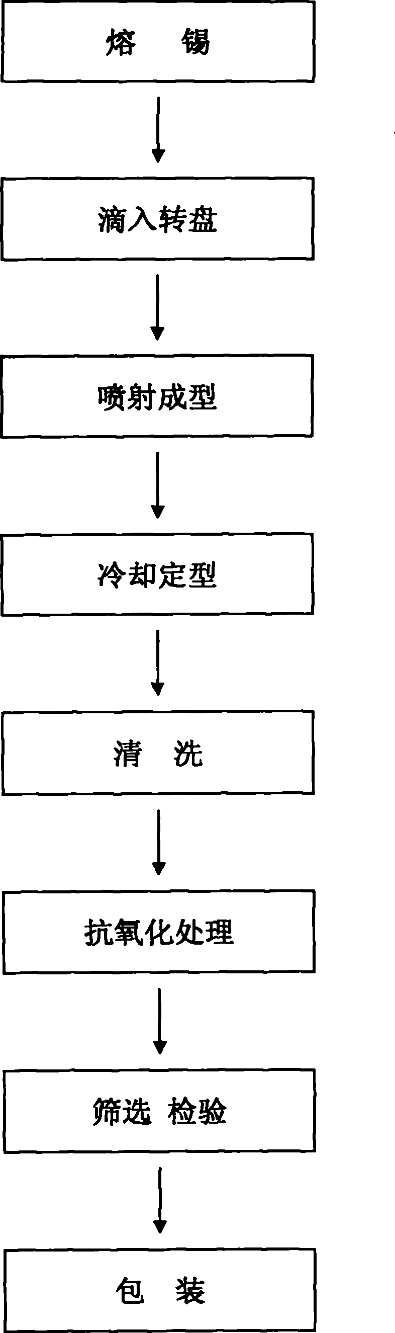
[0024] Such as figure 1 As shown, the production method created by the present invention includes steps such as melting tin, flowing into a turntable, injection molding, cooling and shaping, cleaning, anti-oxidation treatment, screening, inspection, and packaging.

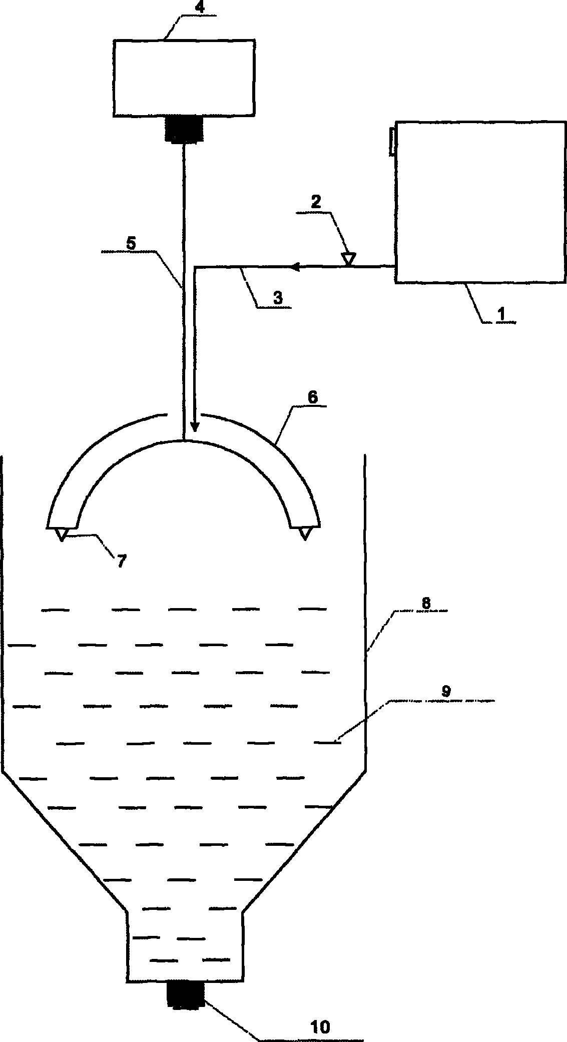
[0025] Such as figure 2 Shown, the equipment that the present invention creates comprises melting furnace 1, pipeline 3, injection molding device, and injection molding device comprises turntable 6, agitator 4, cooling tank 8, coolant 9, and melting furnace 1 is connected to the normal of turntable 6 by pipeline 3 At the top, the tin material is melted in the melting furnace 1 and flows into the turntable 6 through the pipeline. The stirrer 5 is connected to the bottom of the mixer 4. The stirrer 4 is fixed by the inner spherical surface of the stirrer 5 and the turntable 6. The turntable 6 is in the shape of a hemisphere, and a nozzle 7 is installed at the bottom. A cooling tank 8 is provided directly below the ...

Embodiment 2

[0027] The difference between this embodiment and Embodiment 1 lies in that the arc of the turntable 6 in the above equipment is 150°, the width of the inner cavity is 8 cm, and the radius of the outer ball is 20 cm. When producing lead-free solder balls with a ball diameter of 1.0mm, first put the lead-free tin material alloy into the melting furnace 1 to heat and melt, and make the temperature of the tin liquid reach 450°C, open the flow valve 2 to make the tin liquid flow continuously and evenly The rotation speed reaches 1100 rpm and is preheated to 450°C in the turntable 6, and it is ejected from a nozzle 7 with a diameter of 1.1 mm, and falls into a cooling chamber filled with a cooling liquid 9-polyethylene glycol 800 with a temperature of 50°C. 1.0mm lead-free solder ball in the cooling process, and then taken out through the discharge valve 10 at the bottom of the cooling tank 8, the solder ball is cleaned, anti-oxidation treatment, screening, inspection, and then pack...

Embodiment 3

[0029] The difference between this embodiment and Embodiment 1 lies in that the arc of the turntable 6 in the above equipment is 180°, the width of the inner cavity is 10 cm, and the radius of the outer ball is 25 cm. When producing tin-lead alloy tin balls with a ball diameter of 0.1 mm, first put the tin-lead alloy tin ball tin material alloy into the melting furnace 1 to heat and melt, and make the temperature of the tin liquid reach 350°C, and open the flow valve 2 to make the tin liquid continue And evenly flow into the turntable 6 with a rotation speed of 2000 rpm and preheated to 350°C, and spray it out from a nozzle with a diameter of 0.2mm, and fall into the cooling liquid 9-polyethylene glycol with a temperature of 70°C 600 in the cooling tank 8, and during the cooling process, it is shaped into 0.1mm lead-free solder balls, and then taken out through the discharge valve 10 at the bottom of the cooling tank 8, the solder balls are cleaned, anti-oxidation treatment, sc...


PUM

PropertyMeasurementUnit
radiusaaaaaaaaaa
angleaaaaaaaaaa
diameteraaaaaaaaaa

Abstract

The invention discloses tin ball production method and equipment for semiconductor packaging. The method includes feeding tin material into a melting furnace to melt and keeping the temperature of tin liquid at 250-450 DEG C; allowing melted tin liquid to flow into a preheated (preheating temperature and the tin temperature are identical) hemispherical turnplate at rotating speed of 500-3000 rev/min continuously and evenly through a guide pipe; emitting tin balls of uniform sizes from a nozzle of the turnplate to fall into a container carrying cooling liquid to cool and shape; and then washing, performing anti-oxidation treatment, screening, detecting and packaging to obtain products. The tin ball production equipment comprises three parts of the melting furnace, a pipeline and an emitting and shaping device. The manner of continuous feeding is adopted, production rate of the tin balls is increased greatly, and production quantity can be controlled flexibly; produced tin balls are uniform in particle size and high in roundness; and the equipment is simple, operation is facilitated, and production cost is low.

Description

technical field [0001] The invention relates to a production method for producing solder balls with a diameter of 0.1-2.0 mm for semiconductor packaging. The invention also relates to a device used in the above-mentioned production method. Background technique [0002] BGA packaging in semiconductor packaging uses tin balls to replace pins in the IC component packaging structure. BGA packaging can arrange more I / Os. More importantly, it can design from two-layer to multi-layer integrated circuits according to functional requirements. Resistance optimization. The solder balls used in BGA packaging have very high requirements for size and shape accuracy. The existing main technology for producing tin balls is the shred remelting method. First, the tin material is made into tin wire of a certain specification, and then cut into small pieces, which are immersed in a solvent at a certain temperature to melt and solidify into particles. The medium solution causes uneven thickne...

Claims


Application Information

Patent Timeline
Patent Type & Authority Applications(China)
IPC IPC(8): B22F9/10
Inventor 何才雄陈建平李云华汪文珍杨明
Owner 江苏矽智半导体科技有限公司
Why Eureka
Try Eureka