Preparation method of TEM (Transmission Electron Microscope) sample

A sample preparation and sample technology, applied in the field of TEM sample preparation, can solve problems such as TEM sample damage, achieve the effects of improving accuracy, improving analysis quality, and ensuring uniformity

Active Publication Date: 2013-08-21
SHANGHAI HUALI MICROELECTRONICS CORP
View PDF11 Cites 32 Cited by
  • Summary
  • Abstract
  • Description
  • Claims
  • Application Information

AI Technical Summary

Problems solved by technology

[0010] In view of the above-mentioned problems, the present invention provides a method for preparing a TEM sample to overcome the problem in the prior art that the metal protective layer cannot completely fill the high depth when preparing a TEM sample with a semiconductor structure with a high aspect ratio structure or a hole structure. The wide-ratio structure or hole structure leads to the problem of local damage to the TEM sample caused by the ion beam cutting too fast in the edge area of ​​the unfilled hole, and the problem of affecting the quality of TEM analysis due to the poor uniformity of the TEM sample cannot be overcome.

Method used


Image

  • Preparation method of TEM (Transmission Electron Microscope) sample
  • Preparation method of TEM (Transmission Electron Microscope) sample
  • Preparation method of TEM (Transmission Electron Microscope) sample

Examples


Embodiment 1

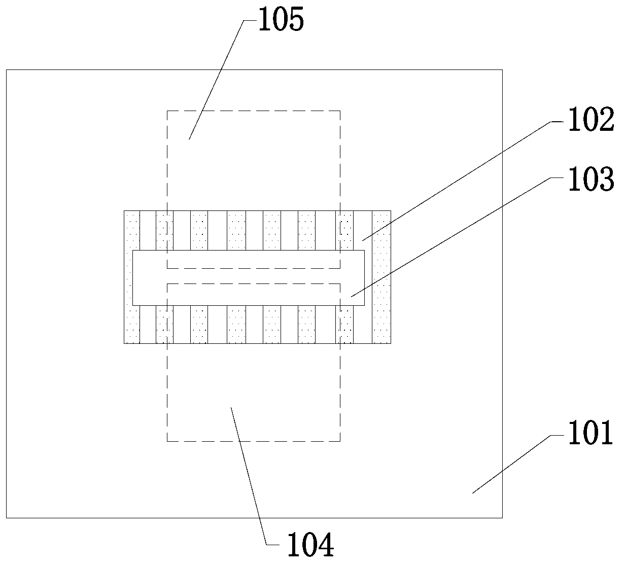
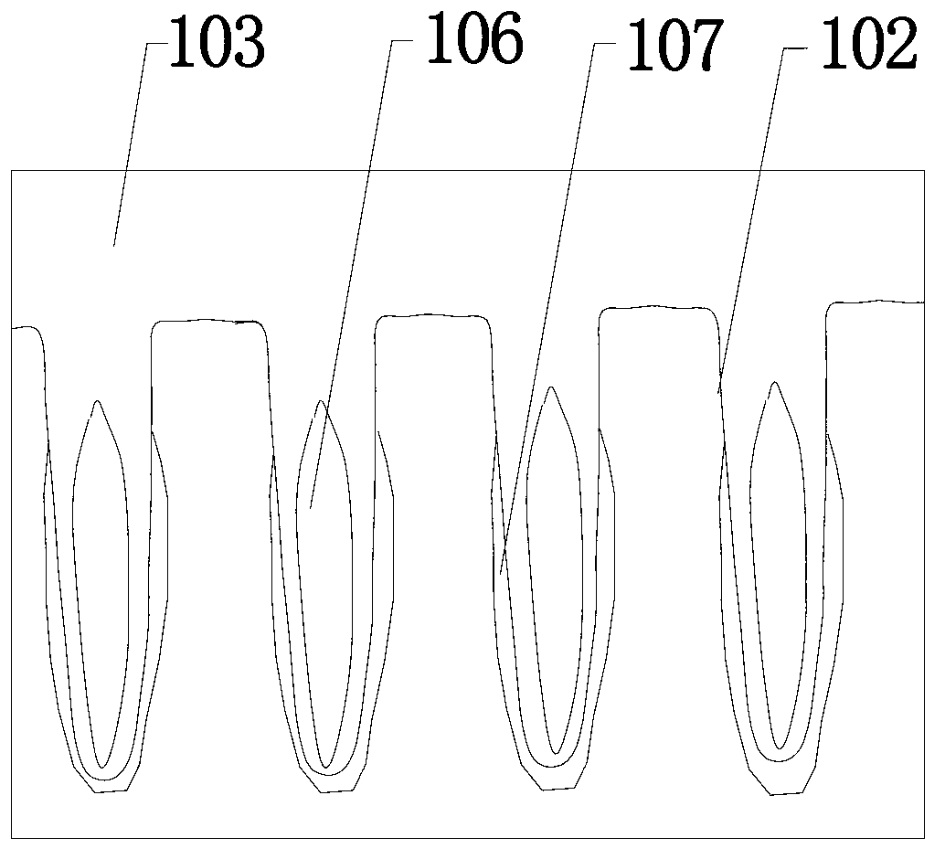
[0047] Figure 4 It is a schematic flow diagram of preparing a TEM sample provided in Embodiment 1 of the present invention; as shown in the figure, firstly, a semiconductor substrate with a trench structure with a high aspect ratio is provided, and a TEM sample preparation region is set on the upper surface of the trench structure, and the The gas-assisted deposition device uses electron beam-assisted deposition or ion beam-assisted deposition to deposit a protective layer on the TEM sample preparation area. The protective layer is a metal protective layer, and its material is Pt or W. The thickness of the metal protective layer is 100nm ~2000nm, such as 100 nm, 150 nm, 300 nm, 700 nm, 1000 nm, 1500 nm, 1900 nm, 2000 nm, etc., and then perform cutting process to prepare TEM sample preparation structure. The cutting process uses Ga ion beam and FIB equipment , and the voltage of the Ga ion beam is 30kv, the current of the Ga ion beam is 50pA~1000pA, such as 50pA, 60pA, 100pA, ...

Embodiment 2

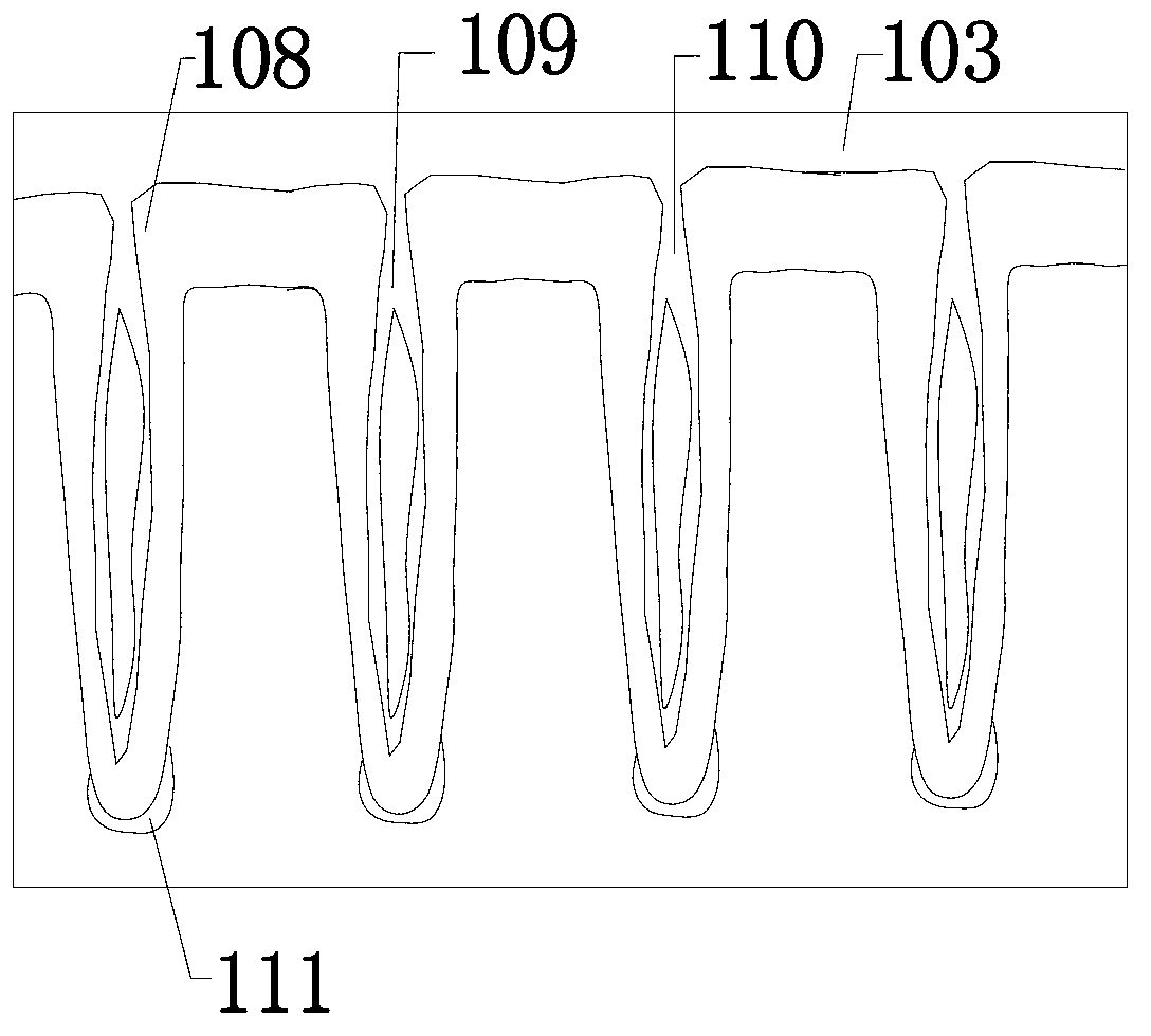
[0060] Figure 12 It is a schematic flow diagram of preparing a TEM sample provided by Embodiment 2 of the present invention; as shown in the figure, firstly, a semiconductor substrate with a trench structure with a high aspect ratio is provided, and a TEM sample preparation region is set on the upper surface of the trench structure, and the The gas-assisted deposition device uses electron beam-assisted deposition or ion beam-assisted deposition to deposit a protective layer in the TEM sample preparation area. The protective layer is a metal protective layer, and its material is Pt or W. The thickness of the metal protective layer is 100nm~ 2000nm, such as 100 nm, 150 nm, 300 nm, 700 nm, 1000 nm, 1500 nm, 1900 nm, 2000 nm, etc., and then perform cutting process to prepare TEM sample preparation structure. The cutting process uses Ga ion beam and uses FIB equipment. And the voltage of the Ga ion beam is 30kv, the current of the Ga ion beam is 50pA~1000pA, such as 50pA, 60pA, 10...


PUM

PropertyMeasurementUnit
thicknessaaaaaaaaaa
thicknessaaaaaaaaaa

Abstract

The invention discloses a preparation method of a TEM (Transmission Electron Microscope) sample. A filling layer is deposited on a preset section in a preparation process of the TEM sample, so that when preparing the TEM sample of a semiconductor structure having a structure with high depth-to-width ratio or a pore structure, local damage of the TEM sample due to overhigh ion beam cutting speed of a non-filled pore edge region generated when a metal protection layer cannot completely fill the structure with high depth-to-width ratio or the pore structure is avoided, and the problem that the bad uniformity of the TEM sample affects the TEM analysis quality is overcome, thus the uniformity of the TEM sample is guaranteed, and further, the analysis quality of the TEM sample is improved, and the observing accuracy of the TEM sample is improved.

Description

[0001] technical field [0002] The invention relates to the technical field of semiconductor manufacturing, in particular to a method for preparing a TEM sample. Background technique [0003] In the semiconductor manufacturing industry, there are a variety of inspection equipment, among which EM is an important tool for inspecting the morphology, size and characteristics of the thin films that make up the device. Commonly used EMs include TEM (Transmission Electron Microscope, transmission electron microscope) and SEM (Scanning Electron Microscope, scanning electron microscope). The working principle of TEM is to thin the sample to be tested by cutting, grinding, ion thinning, etc., and then put it into the TEM observation room, irradiate the sample with a high-voltage accelerated electron beam, enlarge the sample shape, and project it on the screen. , take pictures, and then analyze. One of the outstanding advantages of TEM is that it has a high resolution and can observe...

Claims


Application Information

Patent Timeline
Patent Type & Authority Applications(China)
IPC IPC(8): G01N1/28
Inventor 陈强高林
Owner SHANGHAI HUALI MICROELECTRONICS CORP
Why Eureka
Try Eureka