Preparation method of TEM (Transmission Electron Microscope) sample
A sample preparation and sample technology, applied in the field of TEM sample preparation, can solve problems such as TEM sample damage, achieve the effect of improving accuracy, ensuring uniformity, and improving analysis quality
- Summary
- Abstract
- Description
- Claims
- Application Information
AI Technical Summary
Problems solved by technology
Method used
Image
Examples
Embodiment 1
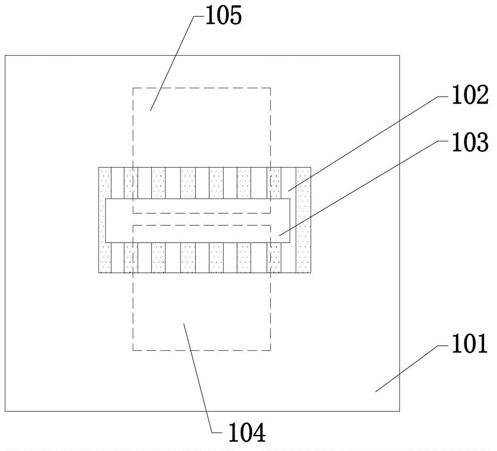
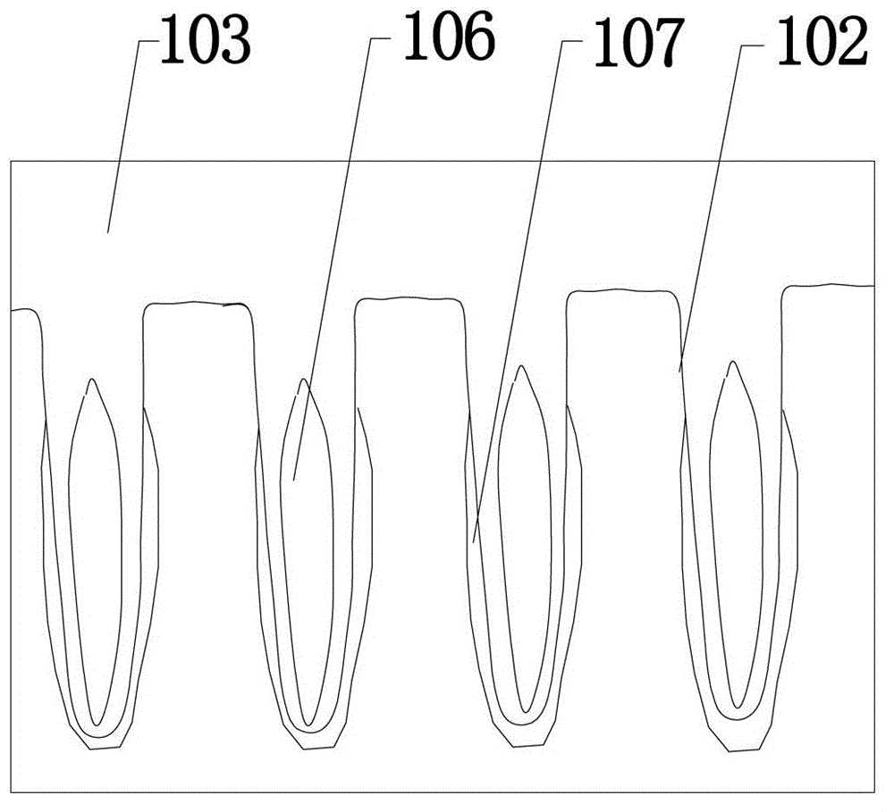
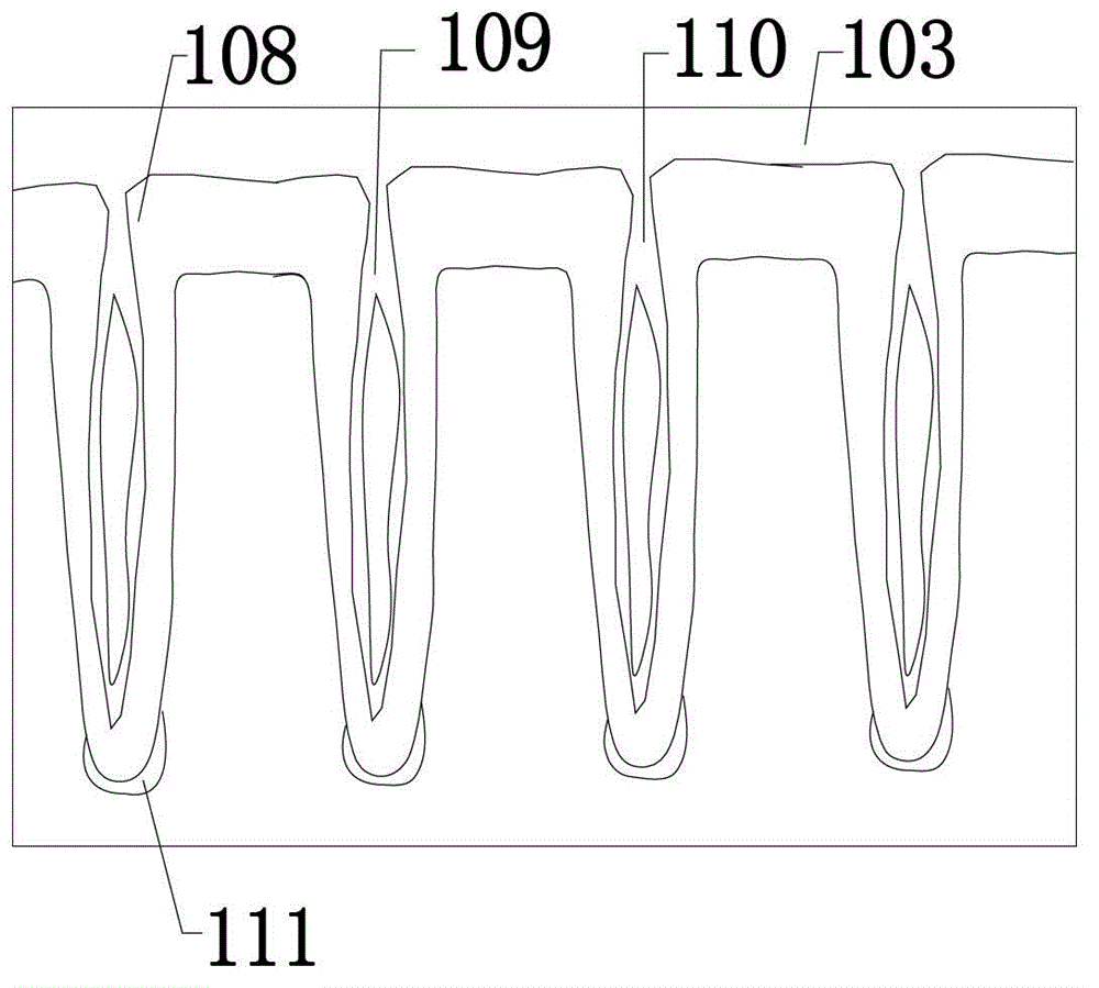
[0046] Figure 4 It is a schematic flow diagram of preparing a TEM sample provided in Embodiment 1 of the present invention; as shown in the figure, firstly, a semiconductor substrate with a trench structure with a high aspect ratio is provided, and a TEM sample preparation region is set on the upper surface of the trench structure, and the The gas-assisted deposition device uses electron beam-assisted deposition or ion beam-assisted deposition to deposit a protective layer on the TEM sample preparation area. The protective layer is a metal protective layer, and its material is Pt or W. The thickness of the metal protective layer is 100nm ~2000nm, such as 100 nm, 150 nm, 300 nm, 700 nm, 1000 nm, 1500 nm, 1900 nm, 2000 nm, etc., and then perform cutting process to prepare TEM sample preparation structure. The cutting process uses Ga ion beam and FIB equipment , and the voltage of the Ga ion beam is 30kv, the current of the Ga ion beam is 50pA~1000pA, such as 50pA, 60pA, 100pA, ...
Embodiment 2
[0059] Figure 12 It is a schematic flow diagram of preparing a TEM sample provided by Embodiment 2 of the present invention; as shown in the figure, firstly, a semiconductor substrate with a trench structure with a high aspect ratio is provided, and a TEM sample preparation region is set on the upper surface of the trench structure, and the The gas-assisted deposition device uses electron beam-assisted deposition or ion beam-assisted deposition to deposit a protective layer in the TEM sample preparation area. The protective layer is a metal protective layer, and its material is Pt or W. The thickness of the metal protective layer is 100nm~ 2000nm, such as 100 nm, 150 nm, 300 nm, 700 nm, 1000 nm, 1500 nm, 1900 nm, 2000 nm, etc., and then perform cutting process to prepare TEM sample preparation structure. The cutting process uses Ga ion beam and uses FIB equipment. And the voltage of the Ga ion beam is 30kv, the current of the Ga ion beam is 50pA~1000pA, such as 50pA, 60pA, 10...
PUM
| Property | Measurement | Unit |
|---|---|---|
| thickness | aaaaa | aaaaa |
| thickness | aaaaa | aaaaa |
Abstract
Description
Claims
Application Information


