Analogue integrated circuit layout designing method capable of improving layout efficiency

A design method and integrated circuit technology, applied in computing, electrical digital data processing, special data processing applications, etc., can solve problems such as unreasonable design, restricting the time to market of integrated circuit products, and reducing layout efficiency, so as to improve circuit performance , improve layout efficiency, and simplify the design process

Active Publication Date: 2013-08-28
EAST CHINA INST OF OPTOELECTRONICS INTEGRATEDDEVICE
View PDF4 Cites 22 Cited by
  • Summary
  • Abstract
  • Description
  • Claims
  • Application Information

AI Technical Summary

Problems solved by technology

The application number is 02158183.5, and the patent application publication titled "Physical Realization Method of Analog Circuit and Radio Frequency Circuit" is designed by this method. The disadvantage of this method is that the splicing is performed after the layout of the module unit is designed. Functional modules and key signals or key devices in functional modules are unreasonably designed. It is necessary to repeatedly modify the designed module layout to meet the performance requirements of the overall circuit, which reduces the layout efficiency and seriously restricts the listing of the entire integrated circuit product. time

Method used


Image

  • Analogue integrated circuit layout designing method capable of improving layout efficiency

Examples


Embodiment 1

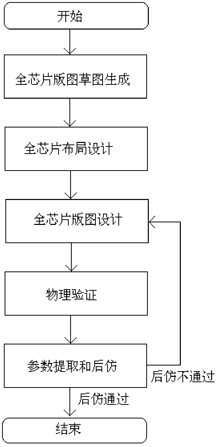
[0018] Embodiment one: see attached figure 1 shown. A method for designing an analog integrated circuit layout that improves layout efficiency, and is used to convert a schematic circuit diagram composed of several modules into a specific physical layout of a full chip. The design method includes the following steps:

[0019] (1) Generation of the physical layout sketch of the full chip:

[0020] Citing the process library devices used in circuit design and using the top-level principle of the circuit to automatically generate the layout of each module in the circuit schematic diagram, and generate a hierarchical full-chip physical layout sketch, the layout of any module includes the layout of all devices in the module , the physical layout sketch of the full chip includes the layout and location of each module;

[0021] (2) Full chip layout design:

[0022] Optimize and adjust the position of the layout of each module in the physical layout sketch of the full chip, and d...


PUM


Abstract

The invention relates to an analogue integrated circuit layout designing method capable of improving layout efficiency. The method includes the following steps: (1) generation of a full-chip physical layout draft: automatic generation of a layout of various modules in a schematic circuit diagram and automatic generation of the hierarchical full-chip physical layout draft by using of process database devices of circuit design according to the circuit top-level principle, (2) full-chip layout design: optimization and adjustment on the position of the layout of the various modules in the full-chip physical layout draft, determination of routes of data lines and routes of signal lines, and optimization and adjustment on positions of key devices in the layout of the various modules, and (3) design of the full-chip physical layout: completion of the final layout design of the various modules, completion of connection of the signal lines among the various modules, then completion of connection of the full-chip signal lines among the various modules, and acquisition of the full-chip physical layout. The analogue integrated circuit layout designing method can improve the layout efficiency and guarantee consistency of parasitic parameters of the devices in technology, circuit and layout design processes, simplifies design procedures, and achieves the purpose of improving circuit performance.

Description

technical field [0001] The invention relates to a design method of an analog integrated circuit layout. Background technique [0002] An analog integrated circuit refers to an integrated circuit that integrates a circuit composed of transistors, resistors, capacitors and other devices on a silicon chip to process analog signals, and generally appears in the form of a hierarchical circuit schematic diagram. After the circuit design is completed, the layout design can be carried out. Layout design is the process of transforming the designed schematic diagram into a specific physical layout. Because the size of the circuit devices contained in the analog integrated circuit varies widely, the structure of the module unit is ever-changing, and the requirements for device and module matching symmetry are high, and the automation of the layout design is very difficult, so the layout design generally adopts a full manual design: first design the layout of the module unit and then s...

Claims


Application Information

Patent Timeline
Patent Type & Authority Applications(China)
IPC IPC(8): G06F17/50
Inventor 吕江萍
Owner EAST CHINA INST OF OPTOELECTRONICS INTEGRATEDDEVICE
Why Eureka
Try Eureka