Method for optimizing superconducting performance of niobium nitride film on silicon substrate by using buffer layer
A technology of superconductivity and niobium nitride, applied in coating, metal material coating process, ion implantation plating, etc., can solve the problem of reduced superconductivity, large lattice mismatch, device service life and stability limitations and other problems, to achieve the effect of improving superconducting performance and obvious effect
- Summary
- Abstract
- Description
- Claims
- Application Information
AI Technical Summary
Problems solved by technology
Method used
Image

Examples
Embodiment Construction
[0014] Below in conjunction with accompanying drawing and specific embodiment, further illustrate the present invention, should be understood that these embodiments are only for illustrating the present invention and are not intended to limit the scope of the present invention, after having read the present invention, those skilled in the art will understand various aspects of the present invention Modifications in equivalent forms all fall within the scope defined by the appended claims of this application.
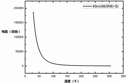
[0015] After substrate cleaning and ion cleaning, a layer of 25-100nm (preferably about 40nm) hexanitrogenpenta-niobium thin film is magnetron sputtered on the high-resistance silicon substrate. The sputtering conditions used are shown in Table 1. Such as figure 1 As shown, we measured the resistance-temperature curve of the prepared niobium hexanitrogen-penta thin film and found that it has semiconductor properties and will not degrade the superconducting properties of ...
PUM
| Property | Measurement | Unit |
|---|---|---|
| thickness | aaaaa | aaaaa |
| thickness | aaaaa | aaaaa |
Abstract
Description
Claims
Application Information