MOS (Metal Oxide Semiconductor) device for ESD (Electrostatic Discharge) protection of integrated circuit chip

A MOS device and integrated circuit technology, applied in the electronic field, can solve the problems of increased device production cost, increased chip area, increased device size, etc., to increase substrate resistance, increase substrate resistance, and improve secondary breakdown The effect of current

Inactive Publication Date: 2013-09-04
UNIV OF ELECTRONICS SCI & TECH OF CHINA +1
View PDF5 Cites 2 Cited by
  • Summary
  • Abstract
  • Description
  • Claims
  • Application Information

AI Technical Summary

Problems solved by technology

However, this method will lead to an increase in the size of the device and an incr...

Method used


Image

  • MOS (Metal Oxide Semiconductor) device for ESD (Electrostatic Discharge) protection of integrated circuit chip
  • MOS (Metal Oxide Semiconductor) device for ESD (Electrostatic Discharge) protection of integrated circuit chip
  • MOS (Metal Oxide Semiconductor) device for ESD (Electrostatic Discharge) protection of integrated circuit chip

Examples


specific Embodiment approach 1

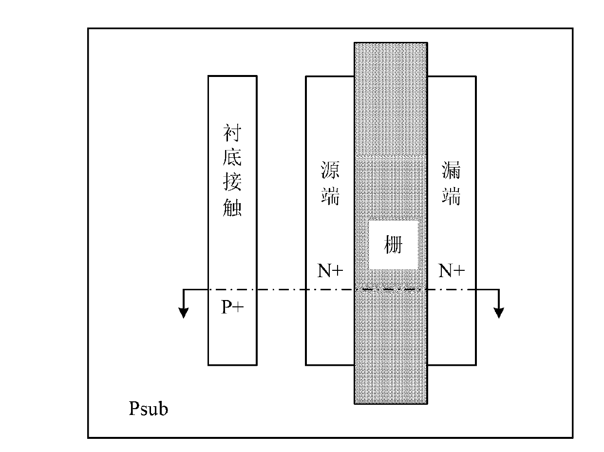
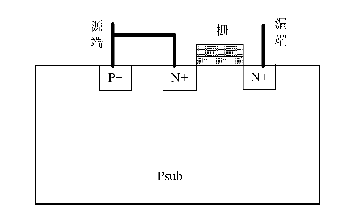
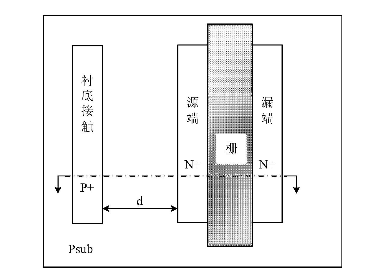
[0020] A kind of NMOS device for integrated circuit chip ESD protection, such as Figure 5 As shown, it includes a P-type semiconductor substrate, a P-type semiconductor source substrate contact region, an N-type semiconductor source region, and an N-type semiconductor drain region; the P-type semiconductor source substrate contact region, N-type semiconductor source region and The N-type semiconductor drain regions are located on the surface of the P-type semiconductor substrate, wherein the P-type source substrate contact region and the N-type semiconductor source region are connected to the source metal, and the N-type semiconductor drain region is connected to the drain metal; the N-type The semiconductor source region is located between the P-type semiconductor source terminal substrate contact region and the N-type semiconductor drain region, and the P-type semiconductor substrate surface between the N-type semiconductor source region and the N-type semiconductor drain re...

specific Embodiment approach 2

[0022] A PMOS device for integrated circuit chip ESD protection, such as Figure 6 As shown, it includes an N-type semiconductor substrate, an N-type semiconductor source substrate contact region, a P-type semiconductor source region, and an N-type semiconductor drain region; the N-type semiconductor source substrate contact region, P-type semiconductor source region and The P-type semiconductor drain regions are all located on the surface of the N-type semiconductor substrate, wherein the N-type source terminal substrate contact region and the P-type semiconductor source region are connected to the source metal, and the P-type semiconductor drain region is connected to the drain metal; the P-type The semiconductor source region is located between the N-type semiconductor source substrate contact region and the P-type semiconductor drain region, and there is a gate oxide layer on the surface of the N-type semiconductor substrate between the P-type semiconductor source region an...


PUM


Abstract

The invention relates to an MOS (Metal Oxide Semiconductor) device for ESD (Electrostatic Discharge) protection of an integrated circuit chip, belonging to the technical field of electronics. On the premise that the size of the device is not increased and more chip area is not required to be consumed, substrate resistance between a source region and a substrate contact region is increased by adding a plurality of strip-shaped well regions which are in parallel with the transverse direction of the device in a substrate region below a position between the source region and the substrate contact region, so that the ESD resisting ability of the device is improved; besides, the size of the substrate resistance of the device can be adjusted and the problem of poor starting uniformity of the device can be solved by adjusting the quantity and the width of the strip-shaped well regions and the mutual distances among the strip-shaped well regions, so that the secondary breakdown current of the device is further improved; meanwhile, the manufacturing process of the MOS device is compatible with the standard CMOS process. In conclusion, the MOS device for the ESD protection of the integrated circuit chip provided by the invention has stronger ESD resisting ability due to the increase of the substrate resistance and the production cost of the device is not increased because the size of the device is not increased.

Description

technical field [0001] The invention belongs to the field of electronic technology, and relates to MOS devices, in particular to MOS devices for protecting semiconductor integrated circuit chips from electrostatic discharge (ElectroStatic Discharge, ESD for short). Background technique [0002] In the process of integrated circuit chip production, packaging, and testing, electrostatic discharge is an inevitable natural phenomenon that is ubiquitous. With the reduction of the feature size of integrated circuit technology and the development of various advanced technologies, it is more and more common for integrated circuit chips to be damaged by ESD phenomenon, which seriously affects the yield rate of integrated circuit chip production. Therefore, major chip production Manufacturers pay more and more attention to the design of anti-static discharge capability of chip integrated circuits. [0003] figure 1 and figure 2 They are the top view and cross-sectional view of a c...

Claims


Application Information

Patent Timeline
IPC IPC(8): H01L29/78H01L29/06
Inventor 张波曲黎明樊航蒋苓利盛玉荣
Owner UNIV OF ELECTRONICS SCI & TECH OF CHINA
Why Eureka
Try Eureka