
A high voltage esd protection device with small hysteresis scr structure of zener breakdown

A technology of ESD protection and zener breakdown, which is applied in the direction of electric solid-state devices, semiconductor devices, electrical components, etc., to achieve the effects of fast response speed, fast turn-on speed, and small on-resistance

Active Publication Date: 2016-07-20
HEFEI IC VALLEY MICROELECTRONICS CO LTD
View PDF5 Cites 0 Cited by
  • Summary
  • Abstract
  • Description
  • Claims
  • Application Information

AI Technical Summary

Problems solved by technology

The high-voltage ESD protection at the interface of the power integrated circuit in the above-mentioned electronic products is a major technical difficulty in the ESD protection design of the entire circuit system
Most of the current high-voltage ESD protection devices are difficult to meet the many requirements of power integrated circuits for high-voltage ESD protection devices: for example, high-voltage ESD protection devices must have a sustain voltage higher than the operating voltage and a breakdown voltage lower than the gate oxide as much as possible trigger voltage, and must also pass the ESD robustness test standard of IEC6001-4-2
In short, the existing high-voltage ESD protection lacks robust ESD protection devices that can meet the narrow ESD window

Method used


Image

  • A high voltage esd protection device with small hysteresis scr structure of zener breakdown
  • A high voltage esd protection device with small hysteresis scr structure of zener breakdown
  • A high voltage esd protection device with small hysteresis scr structure of zener breakdown

Examples


Embodiment Construction

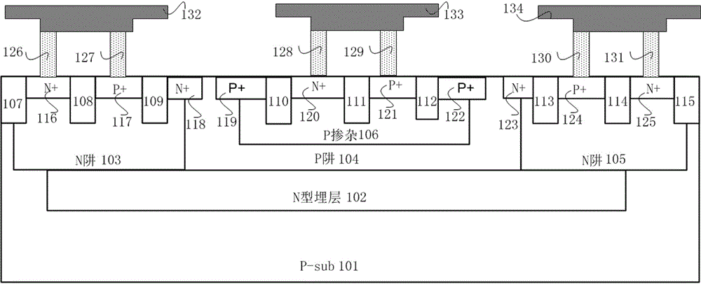
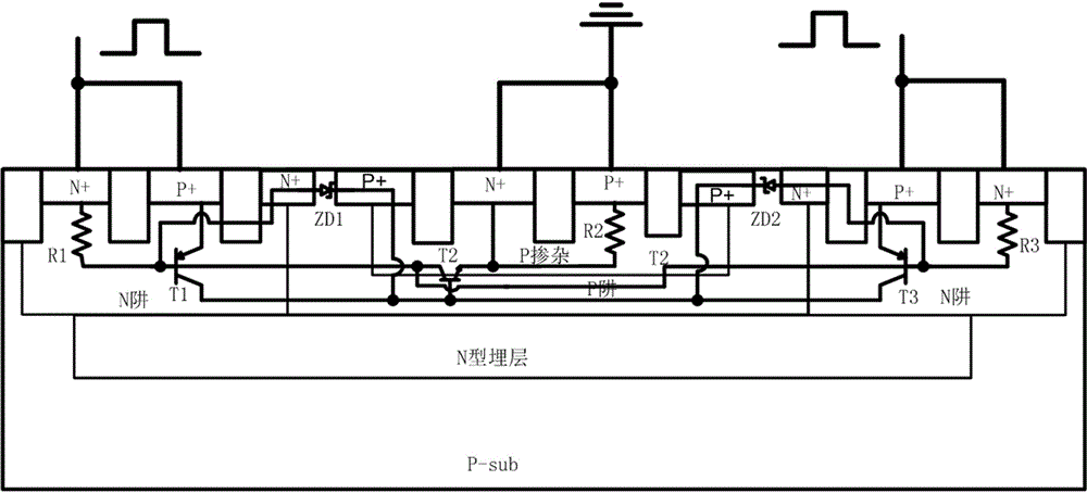
[0025] The present invention proposes a high-voltage ESD protection device with Zener breakdown and small hysteresis SCR structure. Because it is mainly used in the field of high-voltage ESD protection, it needs to be based on a high-voltage BCD process platform, through reasonable design and control of certain features of the device layout parameters, ESD protection devices with different specifications that can meet various high-voltage ESD protection requirements can be prepared. This type of device has two ESD current conduction paths, among which the Zener breakdown circuit structure and the SCR structure with positive feedback mechanism can reduce the trigger voltage of the device, increase the sustain voltage and secondary breakdown current, and also have leakage Small current, small on-resistance, fast response, etc.

[0026] Such as figure 1As shown, it is a structural cross-sectional view of an example device of the present invention, specifically a high-voltage ESD...


PUM


Abstract

A high-voltage ESD protection device with small hysteresis SCR structure of zener breakdown, which can be used for high-voltage ESD protection circuits of on-chip ICs. Including P-type substrate, N-type buried layer, first N well, P well, sinking P doping, second N well, isolation region, first N+, first P+, second N+, second P+, second Three N+, third P+, fourth N+, fourth P+, fifth N+, fifth P+, metal anode, metal cathode. Among them, the first metal anode, metal cathode, first N+, first P+, third N+, third P+, second N+, second P+ or the second metal anode, metal cathode, fifth N+, fifth P+ , the third N+, the third P+, the fourth N+, and the fourth P+ constitute a zener breakdown ESD current discharge path. The Zener breakdown ESD current discharge path can not only enhance the ESD robustness of the device, but also increase the holding voltage of the device, which is suitable for high-voltage ESD protection with a narrow ESD window.

Description

technical field [0001] The invention belongs to the field of electrostatic protection of integrated circuits and relates to a high-voltage ESD protection device, in particular to a high-voltage ESD protection device with small hysteresis SCR structure of Zener breakdown, which can be used to improve the reliability of on-chip IC high-voltage ESD protection. Background technique [0002] With the rapid development of power integration technology, electronic products are increasingly miniaturized, making it easier for people to carry and use them daily. However, with the increasing demand for electronic products such as mobile hard disks, flash memory cards, USB interfaces, and smart phone display touch screens, the reliability problems of integrated circuit products have become increasingly prominent. For example, the data of the flash memory card cannot be read suddenly, the USB interface cannot carry out data communication, and the unreliability problems such as the sudden ...

Claims


Application Information

Patent Timeline
Patent Type & Authority Patents(China)
IPC IPC(8): H01L27/02H01L29/40H01L29/06H01L29/74H01L29/866
Inventor 梁海莲顾晓峰毕秀文董树荣
Owner HEFEI IC VALLEY MICROELECTRONICS CO LTD
Learn More