Method for manufacturing embedded electronic circuit three-dimensional assembly substrate

An electronic circuit and embedded technology, which is applied in the direction of assembling printed circuits, circuits, and electrical solid devices with electrical components, can solve the problems of difficult to guarantee the timing of signal transmission, difficult to achieve technical confidentiality, and difficult to assemble, and to expand the technology. Secrecy way, avoid technology leakage, save space effect

Inactive Publication Date: 2013-09-04
10TH RES INST OF CETC
View PDF6 Cites 8 Cited by
  • Summary
  • Abstract
  • Description
  • Claims
  • Application Information

AI Technical Summary

Problems solved by technology

[0006] The purpose of the present invention is to provide a new design to solve the problems that the timing of signal transmission between devices in the current printed board is difficult to guarantee, and the difficulty of manufacturing and assembling after high density is high, and it is easy to be copied and the technology is not easy to realize. A new method of structural form and electrical interconnection, which can increase the density of interconnection assembly and supplement technical security measures. A method for three-dimensional assembly of embedded electronic circuits on substrates

Method used


Image

  • Method for manufacturing embedded electronic circuit three-dimensional assembly substrate
  • Method for manufacturing embedded electronic circuit three-dimensional assembly substrate

Examples


Embodiment Construction

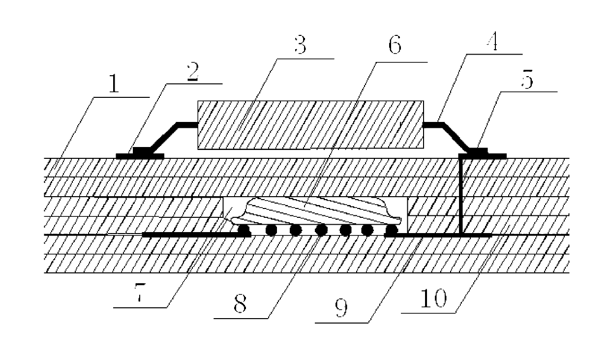
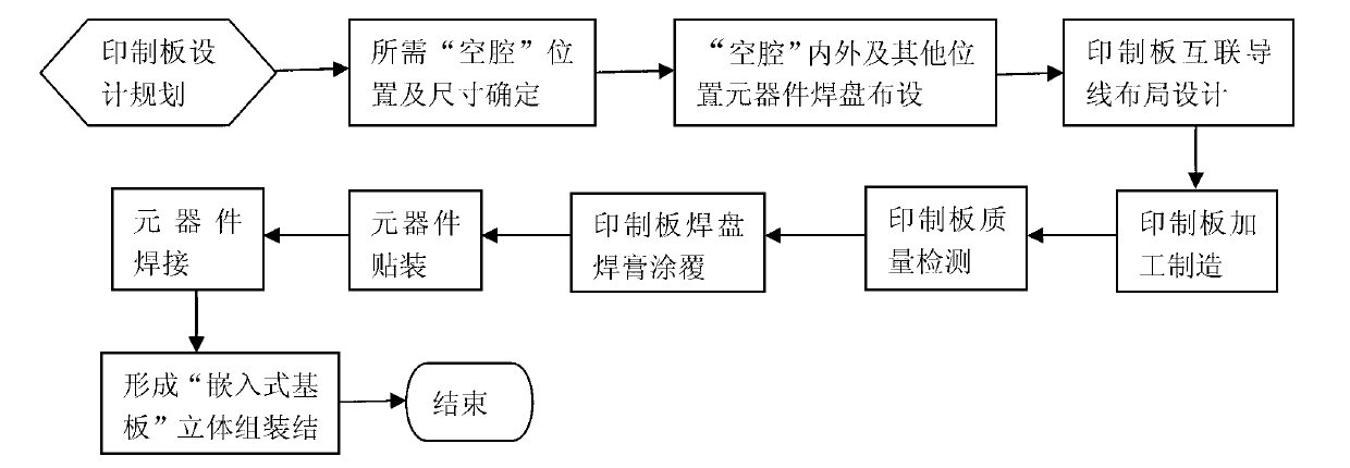
[0022] refer to figure 1 . In the design and manufacturing process of printed circuit components, when designing the layout of printed boards, for some devices, when designing printed boards, according to needs, combined with component packaging, planning and forming printed circuit boards in the printed board substrate 1 Various types of cavities 7 matching the embedded devices in the board, solder joints 8 of embedded components in the printed board, transmission wires 9 in the inner layer of the printed board, and filling materials 10 inside the printed board if necessary. During the manufacturing process of the printed board, the planar printed board is set to be embedded in the embedded substrate, and the cavity 7 whose area and height match the size and height of the layout device and the thickness of the printed board is designed. According to the circuit design, carry out the wiring design and layout of the printed board base material 1, the surface mount device 3, th...


PUM


Abstract

The invention provides a method for manufacturing an embedded electronic circuit three-dimensional assembly substrate, which can be used for increasing the interconnection assembling density and supplementing technical cryptosecurity for the three-dimensional assembly substrate. According to the technical scheme, the method is implemented by the following steps of: in the manufacturing process of a printed board, setting a planar printed board as an embedded substrate, and designing a cavity of which the area and height are matched with the size, height and printed board thickness of a layout device; assembling a device to be embedded on the bottom surface of the cavity in a surface mounting way, or directly laminating and burying into a designed and planed cavity position of the printed board, laminating, connecting a printed lead in the printed board with a device outside the substrate, and covering a printed board substrate with a certain thickness above and below the buried device; and after laminating the printed board, perforating at the pin position of the buried device, performing hole metallization through a buried blind via technique, surface device mounting and through hole insertion to realize interconnection so as to form a three-dimensional laminated assembly structure in which the embedded substrate is taken as a carrier.

Description

technical field [0001] The invention relates to a three-dimensional assembled electronic product board with a high-density, high-reliability three-dimensional structure formed by assembling various semiconductor integrated circuit chips or micro-devices constituting the circuit on a high-density multilayer circuit substrate by using micro-welding and packaging techniques. Level three-dimensional assembly substrate. Background technique [0002] Modern electronic products are developing in the direction of short, small, light, thin and highly reliable, high speed, high performance and low cost, especially airborne, arrow-borne and space-borne electronic products, as well as portable electronic products have a great impact on volume and weight. The requirements for reliability and reliability are becoming more and more stringent. It is required to continuously increase the assembly and interconnection density of circuits, to realize the miniaturization, light weight and high r...

Claims


Application Information

Patent Timeline
Patent Type & Authority Applications(China)
IPC IPC(8): H05K3/34
CPCH01L2224/16225
Inventor 郑国洪郑大安
Owner 10TH RES INST OF CETC
Why Eureka
Try Eureka