Crucible for growing silicon carbide monocrystal and having multiple growth cavities

A silicon carbide single crystal and growth cavity technology, which is applied in the growth of polycrystalline materials, single crystal growth, single crystal growth, etc., can solve the problem of increasing the cost of silicon carbide growth, the high price of silicon carbide wafers, and limiting the size of silicon carbide crystals. issues of scale

Active Publication Date: 2013-09-11
安徽微芯长江半导体材料有限公司
View PDF5 Cites 6 Cited by
  • Summary
  • Abstract
  • Description
  • Claims
  • Application Information

AI Technical Summary

Problems solved by technology

The inherent problem of silicon carbide single crystal growth has greatly increased the cost of silicon carbide growth, making the price of silicon carbide wafer

Method used


Image

  • Crucible for growing silicon carbide monocrystal and having multiple growth cavities
  • Crucible for growing silicon carbide monocrystal and having multiple growth cavities

Examples


Embodiment 1

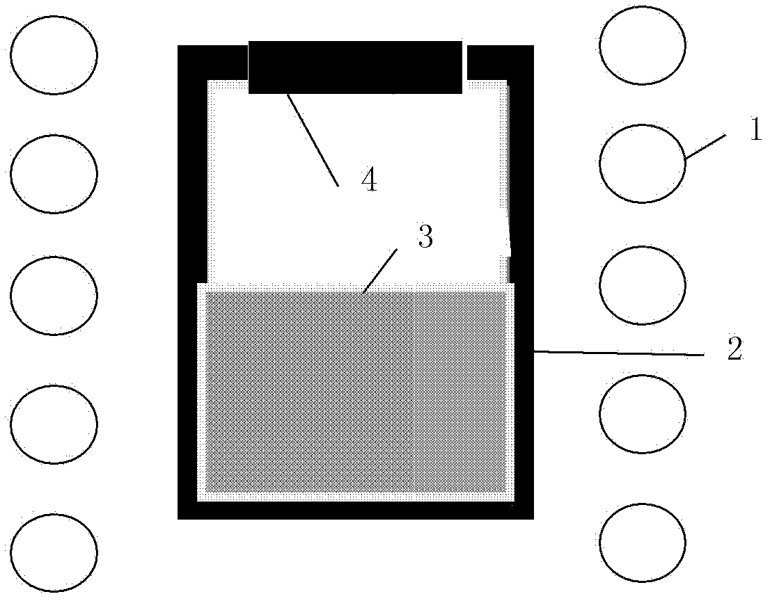
[0026] figure 1 It is the crucible used for growing SiC single crystal by conventional PVT technology. Wherein the thickness of the crucible wall of the crucible cavity is equal.

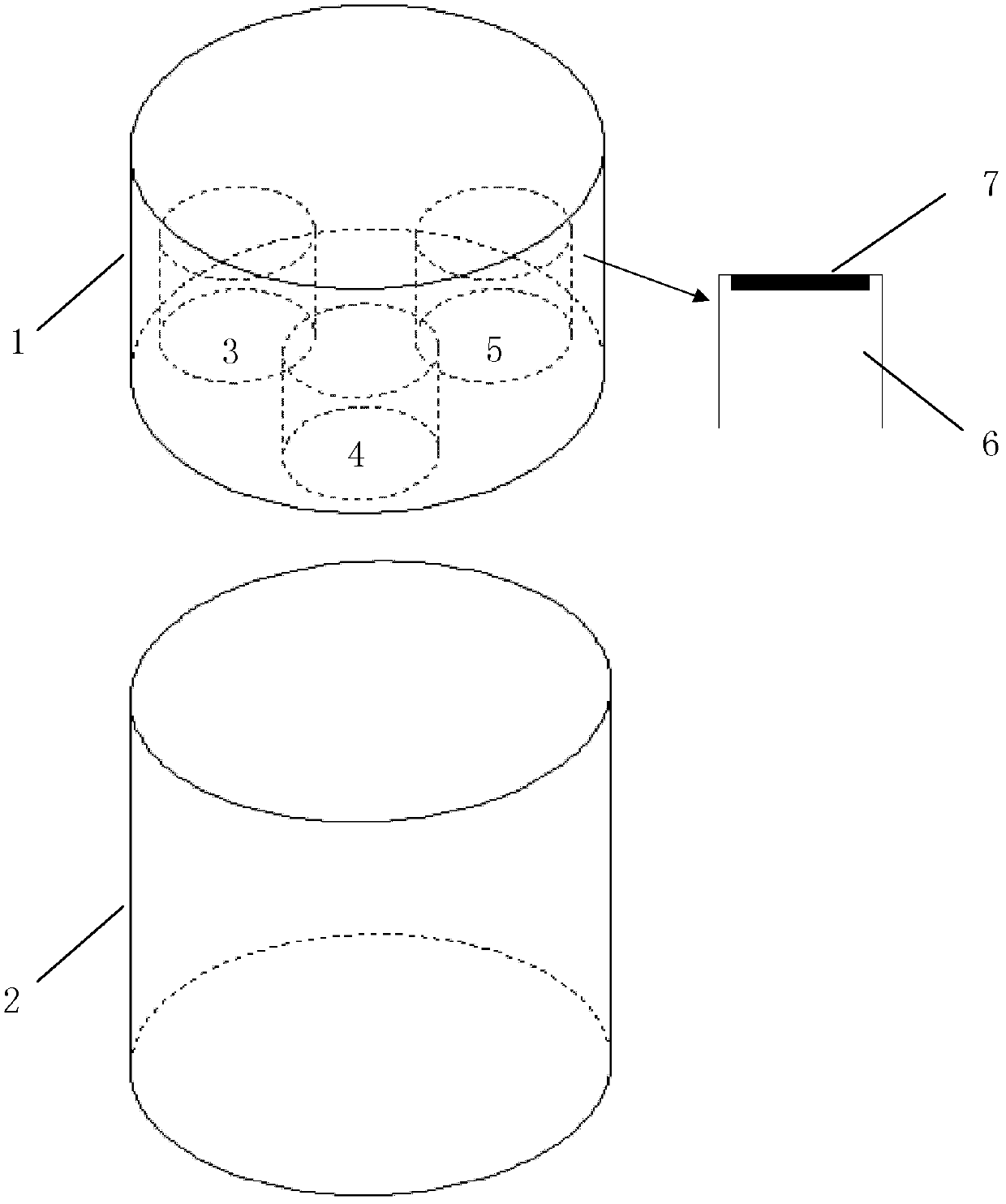
[0027] use figure 2 The crucible design shown is for PVT crystal growth. The crucible is divided into an upper chamber (growth chamber section) and a lower chamber (material chamber). The upper and lower chambers of the crucible (ie, the upper and lower sections) have the same outer diameter of 150 mm. The crucible has 3 independent growth chambers in total, the inner diameter of each growth chamber is 53mm, and the inner diameter of the feeding chamber is 130mm. The thickness of the top cover and the bottom cover of the crucible is 5 mm, and the thickness of the seed crystal holder for installing the seed crystal is 5 mm. The total height of the crucible is 200mm, wherein the height of the growth chamber section is 50mm, and the height of the feed chamber is 150mm. The two parts are connecte...


PUM


Abstract

The invention belongs to the technical field of crystal growth, relates to a crucible structure for growing silicon carbide monocrystals by a physical vapor transport technology, and particularly relates to a crucible for growing silicon carbide monocrystals and having multiple growth cavities. According to the crucible provided by the invention, a material cavity structure of the crucible is in design of multiple growth areas and unified material cavity. The crucible provided by the invention is characterized by adopting the design of multiple growth areas and unified material cavity. In the crucible, multiple silicon carbide monocrystals can be grown synchronously in the same growth period. By adopting the crucible design provided by the invention to grow silicon carbide monocrystals, the growth efficiency can be effectively improved, the growth time is saved, and the crystal cost is reduced. Compared with the traditional method, the monocrystal growth efficiency is improved by 2-3 times on the premise of same equipment configuration.

Description

technical field [0001] The invention belongs to the technical field of crystal growth, and in particular relates to a crucible structure for growing silicon carbide single crystals based on physical vapor transport technology. Background technique [0002] Silicon carbide (SiC) is a compound semiconductor with many excellent properties. Its thermal conductivity is as high as 5.0W / cm (higher than any known metal), so it is very suitable for high temperature and high power electronic devices. In addition, silicon carbide also has high chemical stability and radiation resistance, and has a high degree of lattice matching with GaN. It is an ideal substrate material for manufacturing high-brightness GaN light-emitting diodes. Silicon carbide is a third-generation semiconductor material recognized worldwide. [0003] The synthetic growth technology of silicon carbide crystals has a history of more than 100 years. It can be traced back to 1891. Edward Goodrich Acheson (1856~1931)...

Claims


Application Information

Patent Timeline
IPC IPC(8): C30B29/36C30B35/00
Inventor 忻隽孔海宽严成峰刘熙肖兵杨建华施尔畏
Owner 安徽微芯长江半导体材料有限公司
Why Eureka
Try Eureka