Method for manufacturing thin film transistor and thin film transistor

A technology of thin film transistor and manufacturing method, which is applied in the direction of transistor, semiconductor/solid-state device manufacturing, instruments, etc., can solve the problems of driving integrated circuit IC signal waveform deformation, increasing the driving integrated circuit IC load, time delay, etc.

Active Publication Date: 2013-09-11
SHANGHAI AVIC OPTOELECTRONICS
View PDF4 Cites 4 Cited by
  • Summary
  • Abstract
  • Description
  • Claims
  • Application Information

AI Technical Summary

Problems solved by technology

[0012] In view of this, the object of the present invention is to provide a method for manufacturing a thin film transistor and a thin film transistor to solve the problem of reducing the thickness of the gate insulating layer at the overlapping area of ​​th

Method used


Image

  • Method for manufacturing thin film transistor and thin film transistor
  • Method for manufacturing thin film transistor and thin film transistor
  • Method for manufacturing thin film transistor and thin film transistor

Examples


Embodiment Construction

[0073] In order to make the purpose, technical solutions and advantages of the embodiments of the present invention clearer, the technical solutions in the embodiments of the present invention will be clearly and completely described below in conjunction with the drawings in the embodiments of the present invention. Obviously, the described embodiments It is a part of embodiments of the present invention, but not all embodiments. Based on the embodiments of the present invention, all other embodiments obtained by persons of ordinary skill in the art without making creative efforts belong to the protection scope of the present invention.

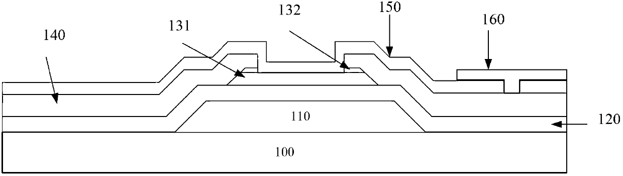
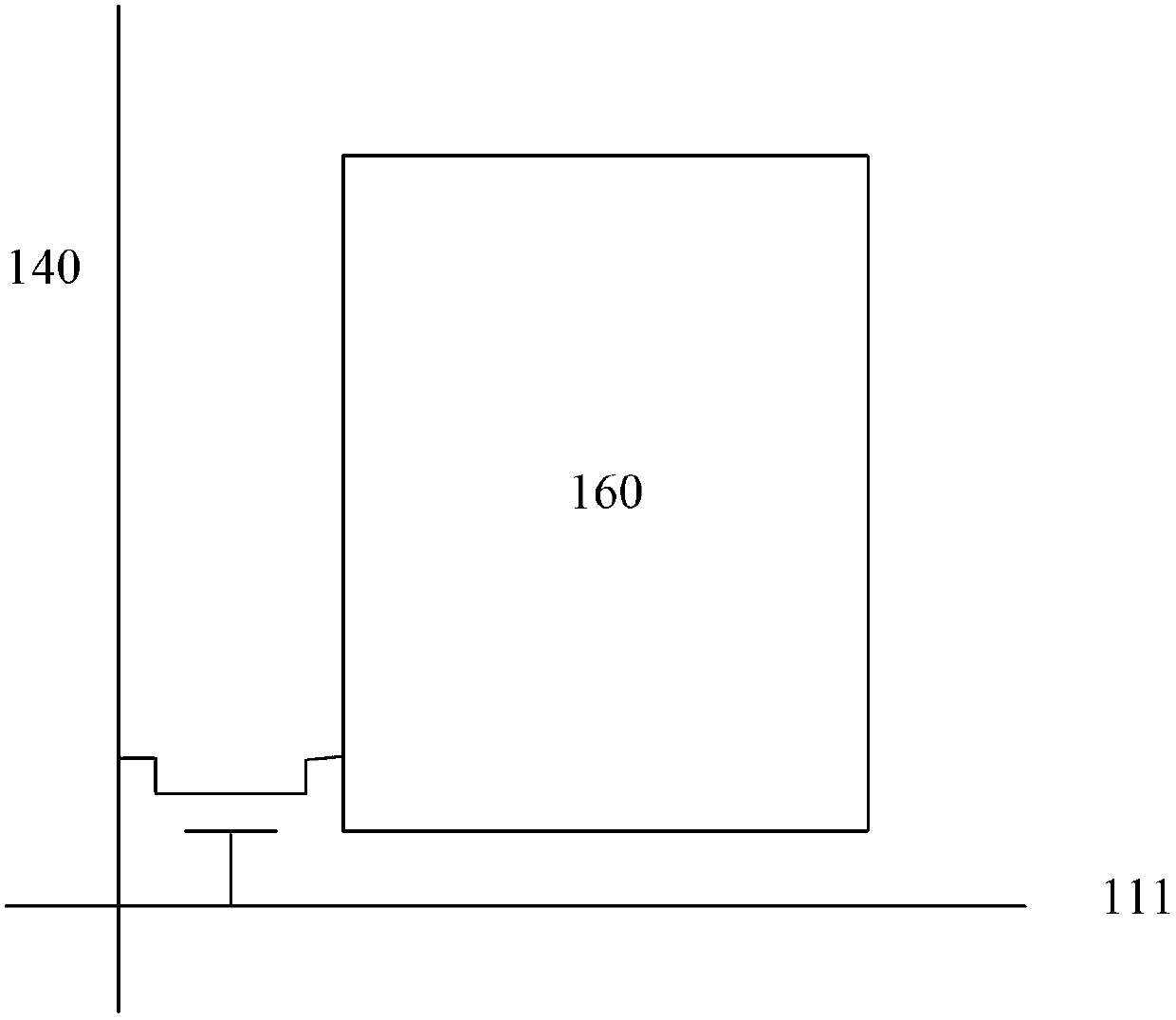
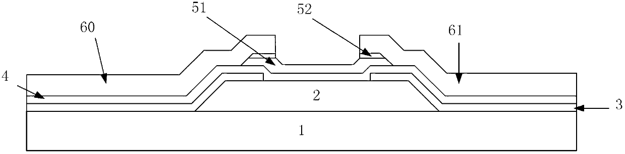
[0074] As mentioned in the background art, in order to improve the driving capability of the transistor in the existing liquid crystal display device, the current intensity can be increased under a fixed voltage, and the thickness of the gate insulating layer above the gate can be reduced. When the thickness of the gate insulating layer outsi...


PUM


Abstract

The invention discloses a method for manufacturing a thin film transistor. The method comprises the steps of providing a substrate, forming the grid electrode of the thin film transistor on the surface of the substrate, depositing a first grid electrode insulating layer on the grid electrode and the surface of the substrate, forming a first grid electrode insulating layer opening in an area above the grid electrode, depositing a second grid electrode insulating layer on the grid electrode and the first grid electrode insulating layer, depositing a semiconductor layer on the surface of the second grid electrode insulating layer to form a silicon island arranged on an area above the grid electrode, and depositing a second metal layer on the silicon island and the surface of the second grid electrode insulating layer to form the source electrode and the drain electrode of the thin film transistor. The thickness of the grid electrode insulating layers is the thickness of the second grid electrode insulating layer in an area with the thickness of a grid electrode insulating film needing to be reduced. The thickness of the grid electrode insulating layers is the superposition of the thickness of the first grid electrode insulating layer and the thickness of the second grid insulating layer in an area with the thickness of the insulating film needing to be increased. The problems of the waveform deformation of signals output by an integrated circuit driving the thin film transistor and time delay can be avoided.

Description

technical field [0001] The invention belongs to the technical field of semiconductors, and in particular relates to a manufacturing method of a thin film transistor and the thin film transistor. Background technique [0002] The information society increasingly needs thin and portable display devices, and the most mature product at present is a liquid crystal display device (Liquid Crystal Display, LCD). A liquid crystal display is composed of a liquid crystal panel and a backlight module. Among them, the liquid crystal panel is composed of an array substrate, a color filter substrate and a liquid crystal layer located between the two substrates, and a full-color display effect can be achieved by means of the color filter. [0003] The array substrate includes a thin film transistor array, such as figure 1 and figure 2 As shown, the existing liquid crystal display device includes: a glass substrate 100, on which a gate 110 and a scanning line 111 are arranged on the surf...

Claims


Application Information

Patent Timeline
IPC IPC(8): H01L21/336H01L29/786G02F1/1362G02F1/1368
Inventor 周思思陈晨
Owner SHANGHAI AVIC OPTOELECTRONICS
Why Eureka
Try Eureka