Formation method of radio frequency components

A technology for radio frequency devices and temporary support, which is applied in the manufacture of electrical solid state devices, semiconductor devices, and semiconductor/solid state devices. big effect

Active Publication Date: 2013-09-11
SHANGHAI HUAHONG GRACE SEMICON MFG CORP
View PDF5 Cites 2 Cited by
  • Summary
  • Abstract
  • Description
  • Claims
  • Application Information

AI Technical Summary

Problems solved by technology

[0005] However, in the actual use process of the above-mentioned silicon-on-insulator radio frequency devices, it will be found that in some radio frequency applications that require high linearity and low insertion loss, there are defects of large signal loss and poor linearity of radio frequency signals.

Method used


Image

  • Formation method of radio frequency components
  • Formation method of radio frequency components
  • Formation method of radio frequency components

Examples


Embodiment Construction

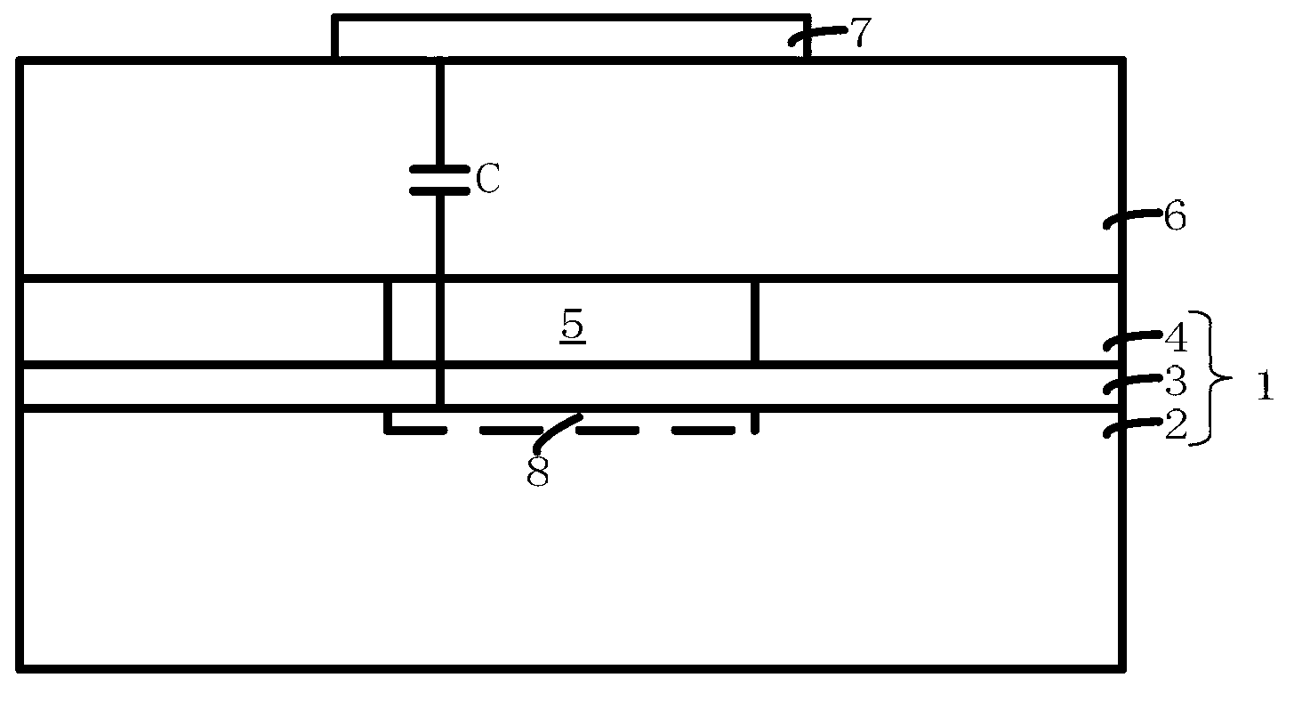
[0025] As mentioned in the background, the radio frequency devices in the prior art have defects of large signal loss and poor linearity of radio frequency signals.

[0026] After research, the inventors found that because the buried oxide layer in silicon-on-insulator is relatively thin, when radio frequency devices are formed on silicon-on-insulator in the prior art, radio frequency signals are still easy to pass through the buried oxide layer, causing loss and affecting linearity. In order to reduce signal loss and improve radio frequency signal linearity, the inventor provides a new method for forming radio frequency devices.

[0027] In order to make the above objects, features and advantages of the present invention more comprehensible, specific implementations of the present invention will be described in detail below in conjunction with the accompanying drawings.

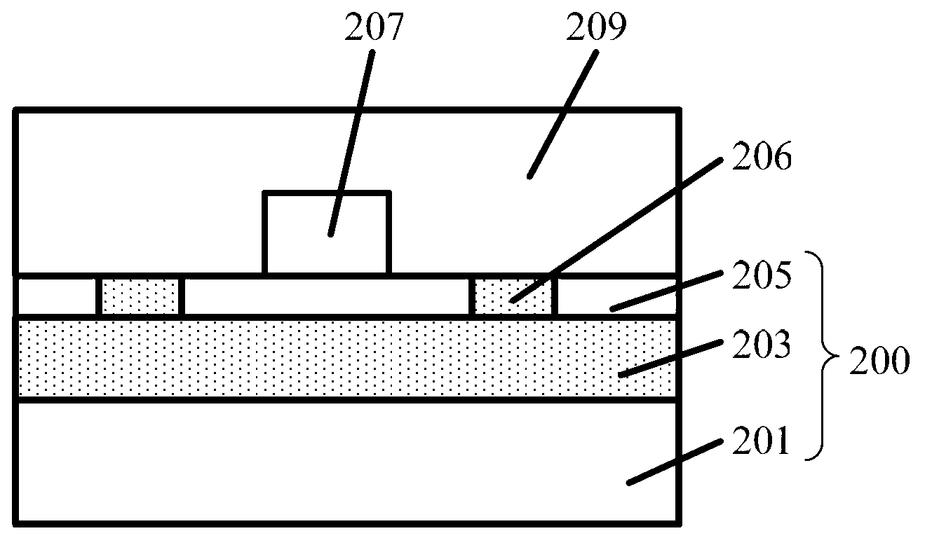
[0028] Please refer to figure 2 , provide a semiconductor-on-insulator layer 200, the semiconductor-on...


PUM


Abstract

A formation method of radio frequency components comprises a back substrate, a buried oxide layer and an upper insulator semiconductor layer. The buried oxide layer covers on the back substrate, and the upper insulator semiconductor layer covers on a top semiconductor layer of the buried oxide layer; a transistor and an interlayer dielectric layer covering on the transistor are formed on the surface of the top semiconductor layer. The formation method includes providing a smooth-surfaced temporary support layer, and jointing the surface of the interlayer dielectric layer and the temporary support layer; removing the back substrate till the buried oxide layer is exposed; providing a high-resistance-rate substrate, and jointing the same with buried oxide layer; removing the temporary support layer to expose the surface of the interlayer dielectric layer after the high-resistance-rate substrate is jointed with the buried oxide layer. By the formation method of the radio frequency components, signal loss is low, and linearity is high.

Description

technical field [0001] The invention relates to the technical field of semiconductor manufacturing, in particular to a method for forming a radio frequency device. Background technique [0002] Semiconductor devices continue to develop toward high integration, high operating speed, and low power consumption. Therefore, the application of bulk silicon (bulk silicon) substrates is increasingly restricted. On the contrary, the silicon-on-insulator substrate has the advantages of realizing dielectric isolation of components in integrated circuits, completely eliminating the parasitic latch effect in bulk silicon CMOS circuits, small parasitic capacitance, high integration density, fast speed, simple process, and small short channel effect. And it is suitable for low-power and low-voltage circuits. Therefore, the use of silicon-on-insulator substrates to form semiconductor devices is becoming more and more popular. [0003] RF devices are required to have a small parasitic capac...

Claims


Application Information

Patent Timeline
Patent Type & Authority Applications(China)
IPC IPC(8): H01L23/66H01L21/683
CPCH01L21/76275H01L21/84H01L29/78603
Inventor 李乐
Owner SHANGHAI HUAHONG GRACE SEMICON MFG CORP
Why Eureka
Try Eureka