
Wafer level packaging structure, method and product for LED flip chip

A wafer-level packaging and flip-chip technology, which is applied to semiconductor devices, electrical components, circuits, etc., can solve the problems of reduced light output efficiency, increased packaging cost, and poor input current uniformity.

Active Publication Date: 2013-09-11
HUAZHONG UNIV OF SCI & TECH
View PDF4 Cites 11 Cited by
  • Summary
  • Abstract
  • Description
  • Claims
  • Application Information

AI Technical Summary

Problems solved by technology

The earliest developed power LED chip is a formal structure, which has serious disadvantages: (1) The thermal conductivity of sapphire is poor, so that the heat of the active layer cannot be dissipated in time, and the temperature of the PN junction is very high; The bottom will absorb the luminescence of the active area, which can only be alleviated by adding a metal reflective layer
(2) Because the two electrodes are on the same side, there is inevitably mutual influence, which makes the uniformity of the input current poor and the electro-optical conversion efficiency decreases
[0003] The traditional packaging method of directly mounting the flip chip on the substrate tends to cause the light emitted from the side to be lost, thereby reducing the light extraction efficiency
Another disadvantage of the traditional surface mount packaging method is that the phosphor coating is difficult to control
In the traditional SMD packaging method, each piece needs to be aligned, and the waste of time increases the cost of the entire packaging, and errors in alignment will also reduce the packaging quality

Method used


Image

  • Wafer level packaging structure, method and product for LED flip chip
  • Wafer level packaging structure, method and product for LED flip chip
  • Wafer level packaging structure, method and product for LED flip chip

Examples


Embodiment Construction

[0031] In order to make the object, technical solution and advantages of the present invention clearer, the present invention will be further described in detail below in conjunction with the accompanying drawings and embodiments. It should be understood that the specific embodiments described here are only used to explain the present invention, not to limit the present invention. In addition, the technical features involved in the various embodiments of the present invention described below can be combined with each other as long as they do not constitute a conflict with each other.

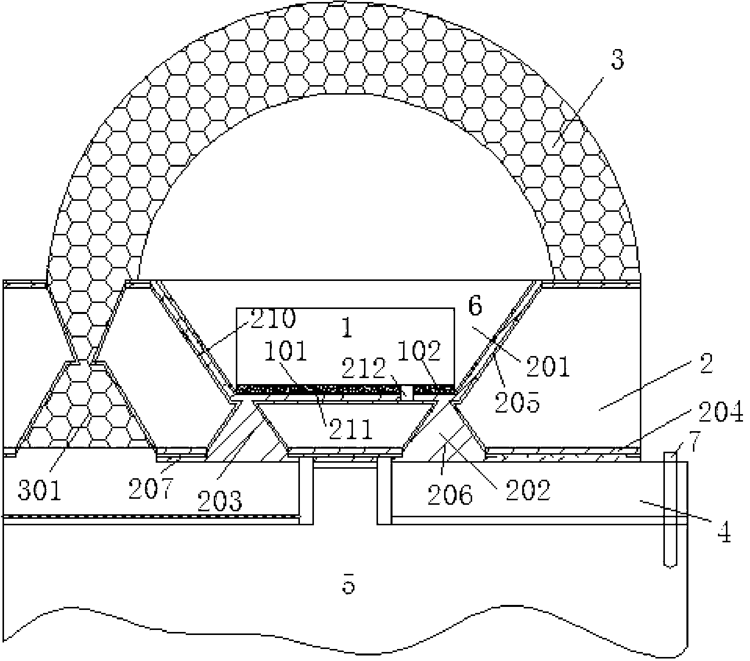
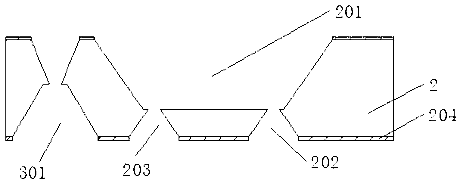
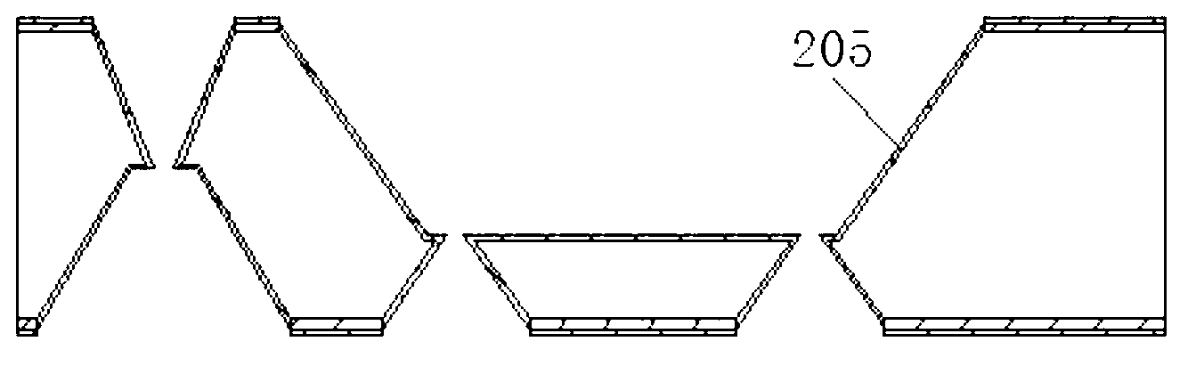
[0032] see figure 1 , a LED flip-chip wafer-level packaging structure of the present invention, comprising LED flip-chip 1 , silicon substrate 2 , lens 3 , printed circuit board 4 and heat sink 5 .

[0033] The surface of the LED flip chip 1 is processed with two electrodes 101 and 102; the front of the silicon substrate 2 is processed with a smooth concave cavity 201 for placing the LED flip c...


PUM


Abstract

The invention discloses a wafer level packaging structure, method and product for an LED flip chip. The wafer level packaging structure comprises the LED flip chip, a silicon substrate, a lens, a printed circuit board and a heat sink. The obverse side of the silicon substrate is provided with a concave cavity in a machined mode, and the concave cavity is used for accommodating the LED flip chip. The length of the bottom of the concave cavity is identical to the length of the LED flip chip. The reverse side of the silicon substrate is provided with two through holes in a machined mode, and the two through holes are communicated with the concave cavity. Insulating layers are deposited on the surface of the concave cavity and the surfaces of the two through holes. A radiating metal layer and a reflecting metal layer are deposited on the insulating layer on the surface of the concave cavity. Metal bodies are filled in the two through holes. The metal bodies in the through holes are connected with the radiating metal layer on the surface of the concave cavity. An opening is formed between two metal layers at the inner bottom of the concave cavity and used for isolating the metal layers into two parts. An insulating layer is deposited on the reverse side of the silicon substrate, and a metal layer is arranged on the surface of the insulating layer in a wiring mode and used for electrode connection. Fluorescent powder is coated in the concave cavity. The periphery of the concave cavity is provided with an annular positioning cavity in a machined mode, and the annular positioning cavity is used for fixing the lens. The wafer level packaging structure, method and product for the LED flip chip can improve LED luminous efficiency, enhance heat dissipation capability and finish self alignment.

Description

technical field [0001] The invention belongs to the technical field of packaging of integrated circuits or discrete devices, and in particular relates to a wafer-level packaging structure, method and product of LED flip chips. Background technique [0002] In recent years, the application of high-power LEDs has attracted a lot of attention due to the improvement of the efficiency of GaN-based LEDs. With the development of lighting technology, high-power white LED will be the core of future lighting. Still, the efficiency of GaN-LED wall sockets on sapphire is only 40% at 350mA, which means that 60% of the energy is converted to heat. In addition, multi-chip high-power LEDs must be packaged into optical devices through bonding. The earliest developed power LED chip is a formal structure, which has serious disadvantages: (1) The thermal conductivity of sapphire is poor, so that the heat of the active layer cannot be dissipated in time, and the temperature of the PN junction ...

Claims


Application Information

Patent Timeline
IPC IPC(8): H01L33/48H01L33/60H01L33/62H01L33/64
Inventor 刘胜吕植成汪学方袁娇娇刘孝刚杨亮陈飞方靖曹斌
Owner HUAZHONG UNIV OF SCI & TECH
Learn More