Laser direct forming process for titanium alloy part
A technology of laser direct forming and process method, applied in the direction of improving process efficiency, improving energy efficiency, etc., can solve problems such as deformation, cracking, poor internal quality, etc., and achieve the effect of reducing manufacturing cost, shortening manufacturing cycle, and high forming efficiency
- Summary
- Abstract
- Description
- Claims
- Application Information
AI Technical Summary
Problems solved by technology
Method used
Image
Examples
example 1
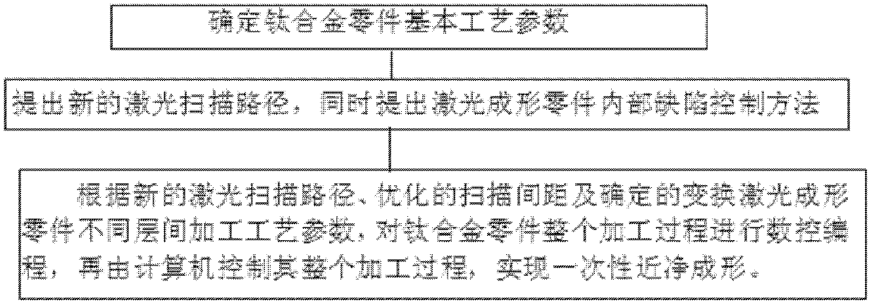
[0028] Such as image 3 Shown is the process flow chart of the laser direct forming titanium alloy parts of the present invention. The present invention is a process method for laser directly forming titanium alloy parts, including the process steps:
[0029] Determine the basic process parameters of titanium alloy parts, and determine the range of forming process parameters of spherical titanium powder through basic process experiments using spherical titanium powder forming materials;
[0030] A new laser scanning path is proposed, and an internal defect control method for laser formed parts is also proposed. This method uses optimized scanning spacing to change the processing parameters between different layers of laser formed parts;
[0031] According to the new laser scanning path, optimized scanning distance and determined transformation of the processing parameters between different layers of laser forming parts, the entire processing process of titanium alloy parts is numeric...
example 2
[0050] The present invention also performs forming processing on connecting parts and corner boxes commonly used in aerospace, forming parts such as Image 6 (b) and Image 6 (c) Shown. These two parts adopt the filling scanning method proposed in the present invention for forming processing. The relevant process parameters adopted are in the process parameters in Table 2. That is, the process parameters used in this embodiment are: laser power 2000-2100W, scanning speed 3-5mm / s, powder feeding rate 0.5~0.9g / min, scanning distance 1.1~1.5mm, layer thickness 0.6~0.8mm. In order to improve the internal organization of the formed parts, the optimized scanning distance and the change of the processing parameters between different layers have been adopted to achieve better results. The other processing techniques are the same as the above.
PUM
 Abstract
Description
Claims
Application Information


